


- News
11 December 2019
JST’s NexTEP program yields bulk GaN crystal growth equipment based on THVPE
The Japan Science and Technology Agency (JST) has developed bulk gallium nitide (GaN) growth equipment based on the tri-halide vapor phase epitaxy (THVPE) method, a development topic of NexTEP (the ‘Newly extended Technology transfer Program’). Development towards commercial application was carried out by the Innovation and R&D Division of Taiyo Nippon Sanso from August 2013 to March 2019, based on the research of professor Akinori Koukitsu of the Tokyo University of Agriculture and Technology. The team has hence developed GaN crystal manufacturing equipment that achieves high speed, high quality and continuous growth.
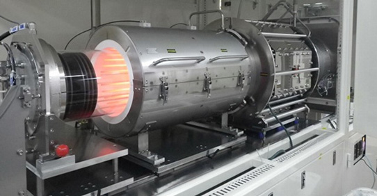
Picture: THVPE crystal growth furnace. ©Taiyo Nippon Sanso Co.
Most GaN substrates used in electronic devices are manufactured using hydride vapor phase epitaxy (HVPE). Compared with other practical vapor deposition methods such as metal-organic chemical vapor deposition (MOCVD) and molecular beam epitaxy (MBE), HVPE offers a faster growth rate (100 microns per hour) together with the benefit of fewer carbon impurities.
However, it is difficult to produce thick GaN crystals using HVPE due to distortions in the crystal, and GaN crystals are grown on a heterogeneous seed crystal substrate, then repeatedly peeled off at a thickness of less than 1mm for use. Commercially practical manufacturing of GaN crystals has hence not been possible so far due to the cost and crystal quality, particularly in the light of the pre- and post-work required in the process, such as cleaning the furnace.
Taiyo Nippon Sanso has advanced the HVPE method to develop a GaN crystal production system that achieves high-speed, high-quality, continuous growth through the tri-halide vapor phase epitaxy method utilizing a gallium trichloride-ammonia reaction system. THVPE succeeds in forming high-quality crystals at a high growth rate three times faster than conventional methods, with only one-fifth the existing density of dislocation defects. The new THVPE method is also said to offer cost advantages over existing techniques, such as not degrading the quartz glass tube of the reactor, avoiding the reduction of crystal growth area, and reducing the occurrence of unnecessary polycrystals.
In particular, when using the standard HVPE method to grow GaN crystals, a particular surface on the crystal will begin growing at a faster rate, and the crystal will continue growing from that surface point as it thickens. The crystal growth area hence decreases as it grows, leading to a turret-like shape. In contrast, THVPE uses the N-polar surface for crystal growth, opposite to the Ga surface. This leads to the reverse phenomenon, and the uppermost growth surface does not decrease even as the crystal grows.
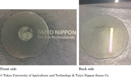
Picture: Front side: transparent - no unnecessary polycrystals are generated on the wafer edge. Back side: since the surface is smooth, the fluorescent light is reflected.
If the THVPE technique can be further developed to achieve production of thick GaN crystals, it should allow the mass production of GaN crystal substrates through slicing. The new technique is reckoned to hold strong promise for achieving a breakthrough in the development of low-cost, high-performance GaN devices.


