


- News
24 December 2019
Hydrogen-terminated diamond transistors on gallium nitride/silicon
École polytechnique fédérale de Lausanne and Lake Diamond SA in Switzerland claim the first p-channel hydrogen-terminated diamond transistors (HTDTs) on gallium nitride (GaN) on silicon templates that demonstrate high-power device performance comparable with other HTDTs on polycrystalline and even monocrystalline diamond [Reza Soleimanzadeh et al, IEEE Electron Device Letters, published online 13 November 2019].
The researchers suggest that integration of p-channel HTDTs with n-channel GaN transistors opens “a pathway for future complementary power switch and logic applications”. The diamond layer is also thermally conductive, allowing improved thermal management of GaN devices in high-power-density applications. The team sees potential for complementary logic operation, gate drivers and complementary power switches in integrated power inverters and converters.
The researchers used an aluminium gallium nitride barrier (AlGaN) GaN-on-silicon template, as used for the fabrication of n-channel high-electron-mobility transistors (HEMTs). The template was prepared for diamond deposition by applying layers of 30nm silicon nitride and 5nm silicon. These layers were designed to protect the template material from the harsh diamond deposition environment, along with enhancing adhesion and thermal conductivity between the materials.
The polycrystalline diamond deposition was seeded with 1-150μm nanoparticles applied in isopropanol solution. The main diamond deposition consisted of microwave-plasma chemical vapor deposition (MPCVD) at 800°C. The plasma power was 3.5kW. The carbon source was 5% methane at 140mbar pressure. Trace quantities of nitrogen and argon were added to improve the growth rate. The carrier gas is not mentioned, but hydrogen is one gas that is used in such processes elsewhere.
Microscopic analysis of the diamond layer showed grains of average size 34μm, smaller than the 100μm grains often reported for the technique. The grains are smaller in the nucleation region, becoming larger at the surface of the 130μm-thick diamond layer.
Further transistor processing (Figure 1) consisted of surface hydrogenation with 650°C 2.8kW hydrogen plasma, deposition of 200nm-thick gold ohmic contacts, wet-etch gold removal from non-contact areas, 800W oxygen plasma treatment to isolate devices, 200°C atomic layer deposition (ALD) of 80nm aluminium oxide as gate oxide and surface termination, and deposition and plasma-etch patterning of 300nm-thick aluminium gate electrode.
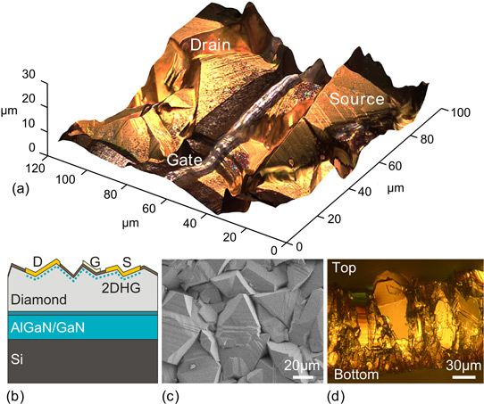
Figure 1: (a) Three-dimensional (3D) optical microscope image of fabricated HTDT, constructed using focus stacking. (b) Schematic of HTDTs. (c) Top-view SEM image of diamond surface. (d) Cross-sectional optical microscope image of diamond layer showing larger grain sizes at top.
The hydrogenation resulted in a p-type conductivity with ~1014/cm2 hole density, according to Hall measurements. The 1.3cm2/V-s mobility resulted in a sheet resistance of 50kΩ/square. The team comments: “The existence of many pits and edges in the unpolished diamond surface, serves as activation sites, resulting in a higher carrier density compared to the commonly reported values in the literature.” The mobility was adversely affected by impurity scattering, the small grain sizes, and the rough surface – values of 3cm2/V-s have been measured for holes in single-crystal diamond.
The fabricated transistor with 4μm gate length achieved an on/off current ratio of 109. The source-gate and gate-drain distances were 2μm and 8μm, respectively. The on-current reached -60mA/mm. The specific on-resistance of 84mΩ-cm2 is described as “low”. The leakage current was “very low” at less than 1μA/mm, even near breakdown.
The breakdown of the device occurred at -400V. The lateral critical field was estimated at 0.4MV/cm, according to studies using isolated contact pads separated by varying distances. The researchers report that monocrystalline diamond has achieved lateral breakdown fields of 1MV/cm.
The effective lateral conductivity came out at 900W/m-K in samples where the silicon substrate was removed from the backside of the diamond/GaN layers. The diamond grain size in the sample was 3μm on average.
The researchers comment: “Such excellent thermal conductivities can lead to very low thermal resistance and robust electrical performances in high-power-density applications. Moreover, this shows the potential of such high-quality CVD-deposited diamond layers for efficient thermal management of high-power GaN devices.”
Comparing the performance with other polycrystalline and monocrystalline devices (Figure 2), the researchers observe that “there is still a gap between the performance of current HTDTs and their theoretical limits, which highlights the significant potential for improvement of this technology.”
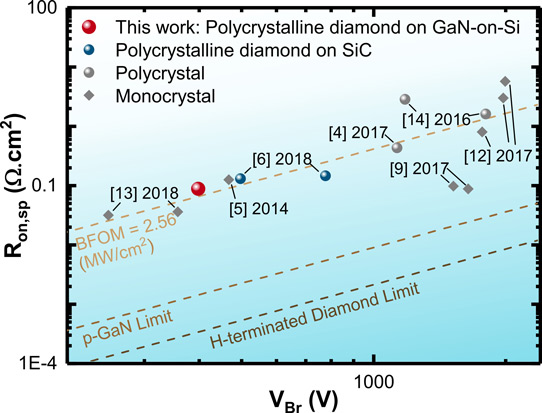
Figure 2: Benchmark of specific on-resistance (Ron,sp) and breakdown voltage (VBr) of this work with heteroepitaxial material on silicon carbide (SiC), as well as polycrystalline and monocrystalline substrate HTDTs.
At the same time, the device exceeds the performance of GaN-based p-channel transistors in terms of “6 times higher current density, 4 orders of magnitude higher on-off ratio and more than 6-times higher thermal conductivity”. The researchers trace the improvement to the higher theoretical Baliga figure of merit of the diamond HTDT structure, compared with p-channel GaN devices.
HTDTs GaN on silicon templates GaN AlGaN HEMTs MPCVD
https://doi.org/10.1109/LED.2019.2953245
The author Mike Cooke is a freelance technology journalist who has worked in the semiconductor and advanced technology sectors since 1997.


