


- News
23 August 2019
UCLA demos first antimonide-based SAM-APDs for x-ray and gamma-ray detection beyond 50keV
A collaborative effort between the University of California at Los Angeles (UCLA) Department of Electrical and Computer Engineering, Department of Molecular and Medical Pharmacology and the California NanoSystem Institute (CNSI) has developed the first antimonide (Sb)-based separate absorption and multiplication avalanche photodiodes (SAM-APDs) that are capable of mapping the energy spectra of x-ray and gamma-ray photons. Under exposure to 241Am radioactive sources, the detectors show photopeaks up to 59.5keV with a full-width half-maximum of 1.283keV (B.-C. Juang et al, Adv. Opt. Mater. 7, 1900107, 2019).
Gamma-rays are generated from the radioactive decay of atomic nuclei. Their energy can range from a few kiloelectron volts (keV) to several Megaelectron volts (MeV), so their application spans many different areas such as astronomy, medical equipment for therapy, sterilization, and radiological security. The UCLA project is funded by the Defense Threat Reduction Agency and US National Science Foundation (NSF).
In these reported detectors, gallium antimonide (GaSb) is used to absorb incoming gamma-rays and excite carriers. Aluminium arsenide antimonide (AlAsSb) is used to make multiplication regions to populate carriers by avalanching (through impact ionization, a breakdown mechanism that can generate very large current, triggered by accelerating a small number of carriers in high electric field and multiplying them). GaSb/AlAsSb SAM-APDs are hence super-sensitive to convert incoming radiation signals into electrical signals.
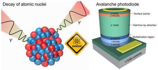
Figure 1. (Left) Gamma-rays arise from decay of atomic nuclei. (Right) Device architecture of GaSb/AlAsSb SAM-APDs.
“Choosing a proper material for the gamma-ray absorption layer is very critical to make high-performance detectors,” says lead researcher Dr Bor-Chau Juang. “We used GaSb because it can offer very good absorption efficiency and efficiently stop high-energy photons due to its high atomic number,” he adds.
“Due to the SAM structure of our detectors, we can get internal gain and thus higher signal-to-noise ratio (SNR). AlAsSb is a large-bandgap semiconductor material and lattice matched with GaSb. We have done lots of device modeling to optimize our detector structure,” says Dr Dingkun Ren, the senior material and device researcher. “Also, there is a large dissimilarity in both pair creation energy and absorption efficiency for GaSb and AlAsSb. As a result, noise photopeaks can be significantly eliminated.”
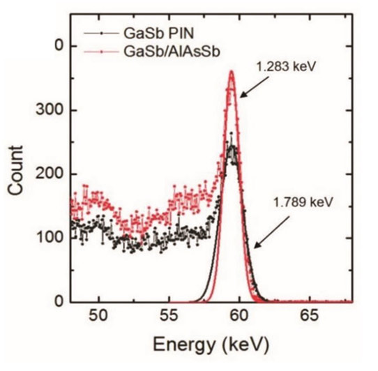
Figure 2. Photopeaks from GaSb/AlAsSb SAM-APDs show higher SNR than those from GaSb photodiodes.
“The GaSb/AlAsSb heterostructures grown by our molecular-beam epitaxy (MBE) system show extremely high quality,” says CNSI technical director Dr Baolai Liang. “The growth parameters were carefully designed,” he adds.
Led by professor Diana L. Huffaker, professor Arion F. Chatziioannou and Dr Baolai Liang, the study paves the way to achieving efficient detection of high-energy photons for x-ray and gamma-ray spectroscopy by Sb-related semiconductor nanostructures. “Our work builds a solid foundation to advance the development of gamma-ray SAM-APDs,” says Liang. “We welcome more collaborations to carry on this research.”
Extremely low-excess-noise and high-sensitivity APDs developed using AlAsSb lattice matched to InP


