


- News
9 August 2019
Annealing to tune output wavelength of quantum dot lasers on silicon
The UK’s University College London and Beijing University of Technology in China have realized indium arsenide (InAs) quantum dot (QD) lasers on silicon with output wavelengths of 1275nm and 1313nm [Mengya Liao et al, Semicond. Sci. Technol., vol34, p085004, 2019].
Selective deposition of silicon dioxide (SiO2) and titanium dioxide (TiO2) before annealing enabled the difference in wavelength by allowing various intermixing of the indium arsenide dots with the surrounding gallium arsenide (GaAs) matrix, tailoring the energy bandgap.
The researchers see the work as potentially enabling silicon-based optical integrated circuits targeting faster transmission speed, higher throughput and lower power dissipation, compared with copper-based information communication systems. QDs are one method for reducing the impact of defects on light emission arising from integration of III-V materials on silicon.
The QDs were grown by molecular beam epitaxy (MBE) on (001) n-type Si offcut 4° in the [110] direction (Figure 1). The dots were grown in well structures (DWELLs) with the InAs dots formed spontaneously from depositing a 2nm InGaAs wetting layer, 3-monolayer InAs and 6nm InGaAs cap. A top layer of dots was found to have a density of 3x10⁸/cm2, according to atomic force microscopy.
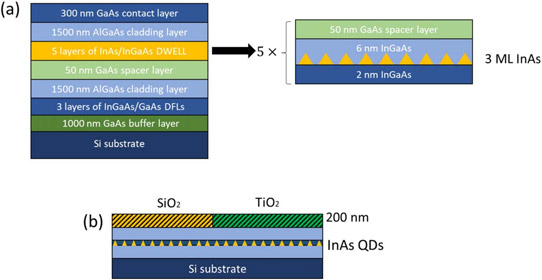
Figure 1: (a) Schematic of InAs/GaAs DWELL laser structure directly grown on silicon substrate. (b) Schematic of SiO2 and TiO2 dielectric layers on III–V/Si QDs for selective-area intermixing.
Threading dislocation density in the active region was suppressed from ~109/cm2 to ~107/cm2 using three five-period InGaAs/GaAs dislocation filter layers (DFLs) as part of the buffer structure. The growth on silicon was initiated using 6nm aluminium arsenide (AlAs) as nucleation for the III-V growth.
Photoluminescence was used to optimize a rapid thermal annealing (RTA) process with silicon dioxide (SiO2) and titanium dioxide (TiO2) top layers. The material used for the optimization study had thinner 100nm cladding layers.
At 700°C, an RTA duration of 30 seconds was found to give the highest intensity with SiO2 cap. The researchers attribute the increase to reduced threading dislocations through interaction and self-annihilation.
The peak wavelength was found to blue shift to shorter wavelengths, from ~1308nm as-grown to ~1294nm with 60-second RTA. The small shift is attributed to intermixing of In and Ga, increasing the bandgap. The full-width at half maximum (FWHM) also tended to narrow as the duration increased, from ~56nm at 5 seconds to ~50nm at 60 seconds. The narrower peaks indicate more homogeneous QD sizes after annealing, according to the researchers.
The 700°C anneal was also found to give the highest PL intensity when the temperature was varied up to 800°C. The team says that, while annealing reduces threading dislocations, annealing at too high a temperature degrades the epitaxial material quality.
Capping with TiO2 before RTA produced somewhat different PL results due to the larger thermal expansion coefficient restricting inter-diffusion rates in the DWELL structure. The highest intensity response was again at 700°C. The blue-shift compared with the as-grown sample was much smaller than for SiO2 capping: ~6.4nm for 30-second RTA at 725°C, compared with ~34nm for SiO2 top layer under the same RTA process.
Broad-area laser bars were produced with platinum/titanium/gold p-type and nickel/germanium-gold/nickel/gold n-type Ohmic contacts. The cavity length was 3mm. The bar width was 25μm. The devices were tested on copper heat-sinks. The facets were not coated. The RTA SiO2/TiO2 capping layers were removed before laser bar fabrication. The RTA process for the fabricated bars was at 725°C for 30 seconds.
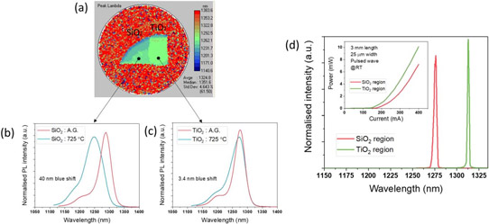
Figure 2: (a) PL mappings of InAs/GaAs DWELL laser sample on silicon for selective-area intermixing at 725°C for 30 seconds. Comparison of PL spectra of InAs/GaAs DWELL laser sample before and after the RTA process in (b) SiO2-capped region and (c) TiO2-capped region. (d) Normalized emission spectra of QD lasers on silicon for as-grown and after RTA under pulsed operation. Inset: light–current QD laser curves for as-grown material and after RTA processes.
The different caps resulted in the lasing peaks which differed by 37nm in wavelength (Figure 2). The threshold currents were 150mA and 175mA for the TiO2- and SiO2-cap devices, respectively. The measurements were made under pulsed conditions with 1μs width and 1% duty cycle. The corresponding output powers (at 400mA)/slope efficiencies were 10mW/0.0563W/A and 7.23mW/0.0499W/A.
The reduced performance with SiO2 cap was attributed to material degradation from intermixing of the InAs and GaAs in the DWELLs.
InAs quantum dot QD lasers InAs GaAs MBE RTA
https://iopscience.iop.org/article/10.1088/1361-6641/ab2c24/pdf
The author Mike Cooke is a freelance technology journalist who has worked in the semiconductor and advanced technology sectors since 1997.


