


- News
22 August 2019
Increasing on-current in III-V transistors on silicon
IBM Research Zurich in Switzerland claims the highest reported on-current for ultra-scaled III-V field-effect transistors (FETs) on silicon [Clarissa Convertino et al, Jpn. J. Appl. Phys. vol58, p080901, 2019]. The gate length was 13nm and the on-current reached 300μA/μm at 0.5V operating voltage, with the off-current at 100nA/μm.
The device used source-drain spacers and doped extension regions to reduce the off-current and mitigate parasitic bipolar and floating-body effects in semiconductor-on-insulator structures. III-V compound semiconductor transistors integrated on silicon platforms are seen as a way to provide future space for the development of radio-frequency and low-power applications.
A 20nm InGaAs layer was transferred to silicon using direct wafer bonding. The 2-inch diameter InGaAs layer was sourced from a metal-organic chemical vapor deposition (MOCVD) process on indium phosphide.
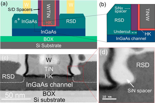
Figure 1: (a) Schematic cross-section of fabricated InGaAs-on-insulator FinFETs. (b) Zoom-in schematic on gate side. (c) Scanning transmission electron microscope (STEM) cross section of 60nm-gate-length device. Dashed line indicates interface between channel and RSD. (d) STEM image on gate side showing 10nm SiN spacers.
The InGaAs layer wafer was bonded to the silicon substrate wafer through silicon dioxide layers deposited on both wafers. The silicon dioxide bond created a 25nm buried oxide (BOX) in the final structure. The indium phosphide was removed by wet etch down to an InGaAs/InAlAs heterostructure that served as an etch stop. A slower wet etch removed the stop layers.
Transistor fabrication began with dry etch of InGaAs fins. A dummy gate was formed by deposition of aluminium oxide liner and amorphous silicon. The amorphous silicon was then patterned and etched with inductively coupled plasma reactive ions (RIE) to give the dummy gate.
Silicon nitride (SiNx) spacers were created using atomic layer deposition (ALD) and RIE. The SiNx spacers were undercut with a hydrochloric acid digital etch process to create an overhang in which doped source/drain extensions are inserted. The tin-doped n+-doped InGaAs raised source/drain (RSD) contacts were then regrown using MOCVD.
Further fabrication consisted of: deposition and chemical mechanical planarization (CMP) of interlayer dielectric; removal of the dummy gate by selective dry etch; plasma-enhanced atomic layer deposition (PE-ALD) of aluminium oxide/hafnium dioxide gate dielectric bilayer and titanium nitride gate metal; sputtering of tungsten (W); CMP; deposition of a second interlayer dielectric oxide; and finishing with a standard level-1 metalization (M1) with source-drain-gate contacts to the devices made through via holes.
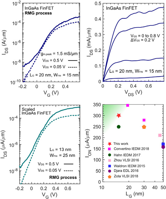
Figure 2: (a) Transfer and (b) output characteristics of InGaAs FinFET with 20nm gate length (LG) and 15nm fin width (WFIN). (c) Transfer characteristic of shortest 13nm-gate-length device. (d) Benchmarking plot showing ION (IOFF at 100nA/μm, VDS at 0.5V) versus LG for different III–V-on-Si technologies. Green-shaded area highlights preferred operation region.
A device with 20nm gate length and 15nm fin width (Figure 2) achieved 350μA/μm on-current (ION) and 100nA/μm off-current (IOFF) at 0.5V drain bias (VDS). The linear and saturation substhreshold swings were 74mV/decade and 78mV/decade, respectively. The researchers claim the on-current is “among the highest for silicon CMOS-compatible III–V FETs”.
The team reports: “In comparison to our previous work, based on devices featuring no spacers, we lower the off-current by approximately three orders of magnitude, resulting in a subthreshold slope improvement near the off-current target and thus an overall increase in ION.”
A 13nm gate length FET (25nm fin width) also achieved a high ION of 300μA/μm with IOFF at 100nA/μm. “This value represents the highest reported on-current for ultra-scaled CMOS-compatible III–V MOSFETs integrated on silicon,” the researchers write.
https://doi.org/10.7567/1347-4065/ab2c97
The author Mike Cooke is a freelance technology journalist who has worked in the semiconductor and advanced technology sectors since 1997.


