


- News
4 July 2018
Hole gas boost for deep ultraviolet diode wall-plug efficiency
US-based Bolb Inc and Semicon Light Co of South Korea have increased efficiency and reduced forward voltage for 280nm-wavelength deep ultraviolet (DUV) light-emitting diodes by creating a two-dimensional hole gas at the p-contact surface using variously strained layers of magnesium (Mg)-doped aluminium gallium nitride (AlGaN) [Jianping Zhang et al, Semicond. Sci. Technol., vol33, p07LT01, 2018].
The hole gas was formed at the surface of a strained heavily doped AlN layer due to strong polarization electric fields, which raised the valence band states above the Fermi level. The electric field arises from the spontaneous charge polarization of the III(Al,Ga)-nitride bond. An added component to the field comes from strain-dependent piezoelectric effects.
The technique is designed to overcome the problem of hole injection from the wider-bandgap high-Al-content AlGaN needed to emit DUV light. Magnesium doping becomes less effective at producing holes as aluminium content increases. And magnesium-doped pure GaN generally has low hole concentrations due to a high activation energy and consequent low activation efficiency of the acceptors into holes. Pure GaN also suffers from having a bandgap narrower than the energy of DUV photons, meaning that its inclusion in such LED structures will absorb the target radiation.
DUV radiation is used to kill germs (among other applications such as curing), and compact, low-cost and efficient LEDs should find application in water purification and food sterilization, avoiding the overuse of antibiotics and the increase in resistant bacteria. Traditional DUV sources contain mercury, which is subject to the Minamata Convention that seeks to eliminate the toxic metal’s use by 2020.
The DUV LED structure was grown on c-plane sapphire by metal-organic vapor phase epitaxy (Figure 1). The p-type layers were kept thin to ensure good hole conduction from the gas into the active multiple quantum well (MQW) region for efficient recombination with electrons into photons.
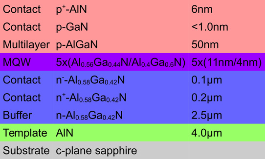
Figure 1: DUV LED epitaxy.
Chips were produced measuring 10milx20mil (0.25mmx0.5mm). The n-contact was made with titanium/aluminium/titanium/gold. Rhodium or palladium was used as p-contact. “It is worth noting that as-deposited Rh or Pd metal layers formed ohmic contacts to the thin heavily Mg-doped AlN layer, indicating high-concentration hole gases forming on the surface of the thin p-type AlN layer,” the researchers write. The p-contact metal was 80nm thick.
The chips were flipped and bonded in 3.5mmx3.5mm ceramic packages. The packages included a half-dome sapphire lens. The rhodium p-contact devices were found to have higher light output due to the metal’s higher reflectance of DUV, compared with palladium.
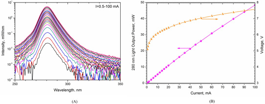
Figure 2: (A) Electroluminescence spectra taken at 0.5-100mA injection from transparent AlN-topped DUV LED. (B) Light output power and voltage characteristics versus current injection.
The light output power at 20mA current injection (55.4A/cm2) was 10.95mW (Figure 2). The forward voltage was 6.43V, a reduction on that of conventional DUV LEDs with a p-GaN hole injection layer. The external quantum efficiency (EQE) and wall-plug efficiency (WPE) were 12.40% and 8.41%, respectively (Figure 3). The light output increased almost linearly up to 48.4mW at 100mA.
Typical WPEs for DUV LEDs with p-GaN contact layers are less than 3%. EQE can be raised to around 10%, and even recently 20%, with the addition of a low amount of Al into the p-GaN, but the WPE is still 5.5-5.7%. The low WPEs are related to low conductivity or to the formation of a Schottky contact, raising the forward voltage.
The researchers estimate that the internal quantum efficiency (IQE) was 83.5% at 12mA injection and 83.0% at 20mA. The light extraction efficiency was put at around 15%. The assessment was based on an approach that uses the different rates for radiative recombination and non-radiative (Auger and Shockley-Read-Hall) recombination to extract IQE from the EQE-current curve. Broader EQE peaks are associated with higher IQE.
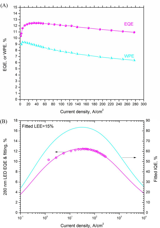
Figure 3: (A) EQE and WPE curves derived from figure 2(B). (B) Carrier recombination model fitting of EQE curve to give IQE and light extraction efficiency (LEE).
The researchers believe that optimization of the device could lead to WPEs of up to 40%. The p-contact using AlN is also expected to benefit other wide-bandgap III-nitride optoelectronics (lasers) and non-optoelectronics (high-temperature, high-power-density bipolar power devices).
DUV light-emitting diodes Mg doped AlGaN AlGaN
https://doi.org/10.1088/1361-6641/aac7c1
The author Mike Cooke is a freelance technology journalist who has worked in the semiconductor and advanced technology sectors since 1997.


