


- News
2 February 2018
IEMN demonstrates over 1400V breakdown on ALLOS’ new GaN-on-Si epi
© Semiconductor Today Magazine / Juno PublishiPicture: Disco’s DAL7440 KABRA laser saw.
A team around Dr Farid Medjdoub at Institut d’Electronique, de Microélectronique et de Nanotechnologie (IEMN-CNRS) research institute in Villeneuve-d'Ascq, France has made devices and conducted measurements on two different gallium nitride on silicon (GaN-on-Si) epitaxial wafer products supplied by IP licensing & technology engineering firm ALLOS Semiconductors GmbH of Dresden, Germany.
One is a prototype of ALLOS’ upcoming product designed specifically for 1200V device applications. With this epiwafer IEMN achieved over 1400V for vertical and 1600V for lateral (grounded) breakdown. The other epiwafer is ALLOS’ established product for 600V applications, which equally showed very high breakdown voltages of 1200V and more for both lateral and vertical measurements.
The new epiwafer for 1200V device applications is from an ongoing internal development program at ALLOS. Its performance results from a structure combining ALLOS’ unique strain-engineering and high-crystal-quality approach with additional measures to suppress leakage and enhance breakdown voltage further. This was achieved without compromising on other essential parameters such as crystal quality or wafer bow and without introducing carbon doping. Epi growth was conducted on a standard Aixtron G5 metal-organic chemical vapor deposition (MOCVD) reactor.
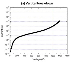
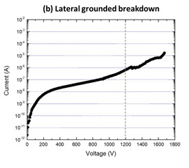
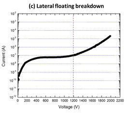
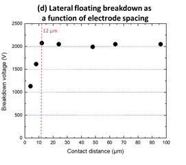
Figure 1(a) to (d): Results from IEMN on ALLOS’ epiwafer technology for 1200V application.
Already at November’s International Forum on Wide Bandgap Semiconductors (IFWS) in Beijing, China, ALLOS presented device results from an industry partner using ALLOS’ 600V epiwafer. With a mature device design and measurement setup for up to 1000V, leakage values of 0.003µA/mm2 at 600V and of 0.033µA/mm2 at 1000V were achieved. The partner’s feedback was “another confirmation for the capability of our technology for 600V applications,” says ALLOS’ chief technology officer Dr Atsushi Nishikawa. “Now the big question was at which voltage above 1000V the physical breakdown occurs and whether we are on track with our development in the 1200V domain too.”
The results demonstrated by IEMN used a simplified device design and processes allowing much faster feedback than from an industrial process. On a prototype of ALLOS’ new epiwafer for 1200V devices, IEMN achieved more than 1400V for vertical and 1600V for lateral (grounded) breakdown voltage (Figure 1(a) and 2(b) respectively). Supplementing characterization with a floating measurement setup resulted in a lateral breakdown of more than 2000V with 12µm contact distance (Figure 1(c)). Saturation of lateral floating breakdown occurred at 12µm contact distance for the 7µm thick epi-stack with breakdown already more than 1100V for 4µm contact distance (Figure 1(d)).
“With over 1400V for vertical and 1600V for lateral breakdown with substrate grounded, ALLOS’ epiwafer favorably compares to all the samples we have measured so far from various industry and research partners,” comments IEMN’s GaN team leader Dr Farid Medjdoub. “Furthermore, the results we have seen indicate that the device performance is very uniform over the wafer, which is a very important characteristic to qualify for actual device production.”
On ALLOS’ 600V epiwafer, IEMN achieved 1200V for vertical and 1500V for lateral (grounded) breakdown voltage. Both epiwafer products are not doped with carbon, which is often used by GaN-on-Si makers to enhance isolation but has negative impacts on crystal quality and dynamic switching behavior. Both are available with 675µm thickness for 150mm wafer diameter and 725µm thickness for 200mm. Bow for all ALLOS epiwafer products is tightly controlled to below 30µm.
“The results now available show that we are already at 1.7MV/cm laterally and 2MV/cm vertically – and we have a program to realize further improvements on the epiwafer level,” says ALLOS’ CEO Burkhard Slischka. “Now is the time to establish a strong partnership with an industrial partner also in the 1200V product range,” he adds. “As we are a pure epiwafer technology provider without own device making we are seeking a close cooperation with an experienced power electronics player to exploit the opportunities for their 1200V GaN-on-Si based applications. With our technology, GaN-on-Si has the potential to effectively compete with SiC performance at a fraction of the wafer cost.”
ALLOS challenges conventional beliefs of GaN-on-Si
ALLOS' doping-free 600V HEMT epi technology running on both Aixtron G5 and Veeco K465i at customer
ALLOS transfers GaN-on-Si power semiconductor epi technology to customer


