


- News
4 December 2018
EVG unveils BONDSCALE fusion wafer bonder for ‘More Moore’ scaling and front-end processing
EV Group of St Florian, Austria – a supplier of wafer bonding and lithography equipment for semiconductor, micro-electro-mechanical systems (MEMS) and nanotechnology applications – has introduced the all-new BONDSCALE automated production fusion bonding system, designed for a wide range of fusion/molecular wafer bonding applications, including engineered substrate manufacturing and 3D integration approaches that use layer-transfer processing, such as monolithic 3D (M3D).
The firm says that BONDSCALE brings wafer bonding to front-end semiconductor processing and helps to address long-term challenges for ‘More Moore’ logic device scaling identified in the International Roadmap for Devices and Systems (IRDS). Incorporating enhanced edge-alignment technology, BONDSCALE is claimed to provide a significant boost in wafer bond productivity and lower cost of ownership (CoO) compared with existing fusion bonding platforms.
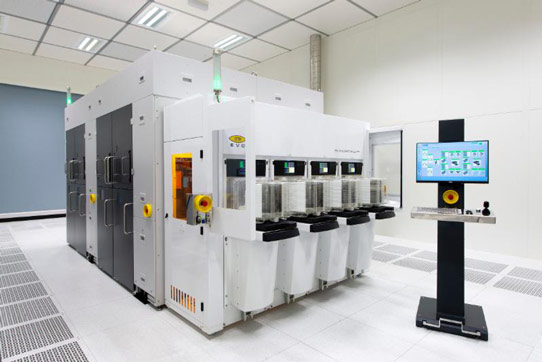
Picture: BONDSCALE automated production fusion bonding system.
Already being shipped to customers, BONDSCALE is being sold alongside EVG’s GEMINI FB XT automated fusion bonding system, with each platform targeting different applications. While BONDSCALE will primarily focus on engineered substrate bonding and layer-transfer processing, the GEMINI FB XT will support applications requiring higher alignment accuracies, such as memory stacking, 3D systems on chip (SoC), backside illuminated CMOS image sensor stacking, and die partitioning.
Direct wafer bonding key to driving semiconductor performance scaling
According to the IRDS Roadmap, parasitic scaling will become a dominant driver of logic device performance in the coming years, requiring new transistor architectures and materials. The roadmap also notes that new 3D integration approaches such as M3D will be necessary to support the long-term transition from 2D to 3D VLSI, including backside power distribution, N&P stacking, logic-on-memory, clustered functional stacks and beyond-CMOS adoption. Layer-transfer processes and engineered substrates are enabling technologies for logic scaling by helping to deliver significant improvements in device performance, functionality and power consumption. Direct wafer bonding with plasma activation is a proven solution for enabling heterogeneous integration of different materials, high-quality engineered substrates as well as thin-silicon-layer-transfer applications.
“Nearly 25 years ago, EVG introduced the industry’s first silicon-on-insulator (SOI) wafer bonder to support the production of high-frequency and radiation-hard devices for niche applications,” says executive technology director Paul Lindner. “Since then, we have continuously enhanced the performance and CoO of our direct bonding platforms to help our customers bring the benefits of engineered substrates to a wider range of applications,” he adds. “Our new BONDSCALE solution takes this to the next level, boosting productivity to fulfill the growing need for engineered substrates and layer-transfer processing to enable continued performance, power and area scaling of next-generation logic and memory devices in the ‘More Moore' era.”
BONDSCALE is a high-volume production system for fusion/direct wafer bonding needed for front-end-of-line applications. Featuring EVG’s LowTemp plasma activation technology, it combines all essential steps for fusion bonding - including cleaning, plasma activation, alignment, pre-bonding and IR inspection - in a single platform suitable for a wide range of fusion/molecular wafer bonding applications. Capable of processing both 200mm and 300mm wafers, the system ensures a void-free, high-throughput and high-yield production process, says EVG.
BONDSCALE incorporates next-generation fusion/direct bonding modules, a new wafer handling system and optical edge alignment to provide higher throughput and productivity to support the ramp up of engineered substrate wafer production and M3D integration.


