


- News
22 August 2018
Agnitron develops MOCVD capability for 10kV+ beta-phase gallium oxide switches
© Semiconductor Today Magazine / Juno PublishiPicture: Disco’s DAL7440 KABRA laser saw.
At the 3rd US Workshop on Gallium Oxide (GOX 2018) at Ohio State University, Columbus, Ohio (15-16 August), Agnitron Technology Inc of Eden Prairie, MN, USA presented a new metal-organic chemical vapor deposition (MOCVD) growth capability that is said to deliver an order-of-magnitude improvement to background concentration levels for beta-phase gallium oxide (β-Ga2O3) films.
The development has resulted in a new record, regardless of deposition technique, for room-temperature and low-temperature bulk film mobilities in β-Ga2O3. This advance is key to realizing the potential of the material system for operating at high voltages – an application with broad interest for the 4.9eV-bandgap semiconductor. Calculations indicate that this new capability can support the fabrication of field-effect transistor devices capable of operating beyond 10kV.
β-Ga2O3 and other wide-bandgap semiconductors exhibit material properties that can allow power electronic switches to improve performance in various aspects, i.e. lower on-resistance and switching losses, higher operating temperatures, and higher-frequency operation. If realized, these improvements will allow many types of voltage converter systems to reduce size, weight and complexity while improving energy efficiency. Over time this could translate to improved performance and tremendous energy savings on a large scale for electric drive vehicles, transportation infrastructure and distributed/renewable energy systems, among others.
The Agnitron team, led by its president Dr Andrei Osinsky as the program’s principal investigator, hence recently performed a series of experiments to better understand how good MOCVD-grown β-Ga2O3 films can be. “It was clear that reducing background concentration is critical to the future commercial viability of β-Ga2O3. Thus, we focused on optimizing a number of key reactor and process parameters and managed to grow films with surprisingly low levels,” says Osinsky. “Already a number of recent runs have produced films near 10µm thick and shown the improved process can reproducibly offer background concentration levels in the ~5E15cm-3 range, as measured by CV and Hall measurement techniques,” he adds. The lowest concentration measured to date was by CV with an Nd – Na value of 3E15cm-3. These low background concentrations have led to the observation of electron mobilities in the films at room temperature and low temperature of 174cm2/(V·s) and 2800cm2/(V·s), respectively – new records for the material based on published literature. The films have also been produced with surface roughness levels <0.2nm root-mean-square (RMS) – a key property for both lateral and vertical conducting devices.
Over the last two years professor James Speck of University of California Santa Barbara (UCSB) has collaborated with Agnitron on multiple β-Ga2O3 projects, and his group performed measurements on the reported films. “This new capability by Agnitron sets yet another record for β-Ga2O3 mobilities by MOCVD or any technique,” comments Speck. “It is a critical development for pushing voltage performance of power transistors higher and opens the door for a number of device types.”
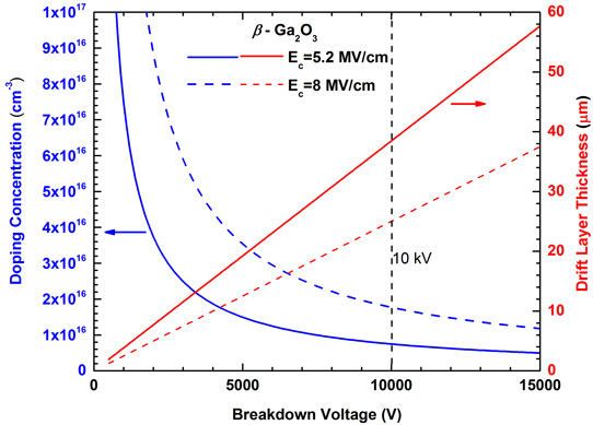
Figure 1. Doping concentration (blue traces) and drift layer thickness (red traces) versus breakdown voltage for β-Ga2O3. Solid lines are for β-Ga2O3 layer with critical breakdown field of 5.2MV/cm (experimentally demonstrated by Cornell University). Dashed lines are for β-Ga2O3 layer with the theoretical critical breakdown field of 8MV/cm. The vertical dashed line shows the doping concentration and the drift layer thickness needed to realize power devices that operate at a voltage of 10kV. Calculations and plot courtesy of professor Huili (Grace) Xing of Cornell University.
A number of important device properties dictate the ultimate voltage performance of a field-effect transistor. These include but are not limited to the film material properties and the dimensions and background impurity concentration of the drift layer/region. The background impurity concentration also directly influences the electron mobility of the films for all device topologies (generally requiring fewer impurities to achieve higher electron mobility). Since β-Ga2O3 exhibits a breakdown field well beyond that of silicon, silicon carbide (SiC) and gallium nitride (GaN), β-Ga2O3-based devices can potentially be thinner or smaller while operating at the same voltages as these other materials or go to levels not otherwise possible. Calculations indicate that a background concentration in the range now available from Agnitron’s MOCVD process (~5E15cm-3 range) will support device operation beyond 10kV, as shown in Figure 1 – a new voltage performance class for field-effect transistor devices.
Agnitron’s ongoing β-Ga2O3 development work is in part supported by US Office of Naval Research (ONR) contract number N6833518C0192 (under the direction of Lynn Peterson) and Air Force Research Laboratory (AFRL) contract number FA9550-17-P-0029 (under the direction of Dr Ali Sayir).
https://leconference.weebly.com/gallium-oxide-workshop.html


