


- News
4 July 2017
AP&S triples size of in-house application laboratory, forming Demo Center
AP&S International GmbH of Donaueschingen, Germany (which designs and produces batch- and single-wafer wet process equipment for surface treatment of substrates under cleanroom/sterile conditions) says that, after making a significant investment in the expansion and modernization of its in-house laboratory in 2016, its size has now almost tripled – from 23m³ originally to 66m³ after the renovation. Since reopening this year, the modified laboratory (the firm’s new Demo Center) is open to customers worldwide, offering a variety of single-wafer process demonstrations.
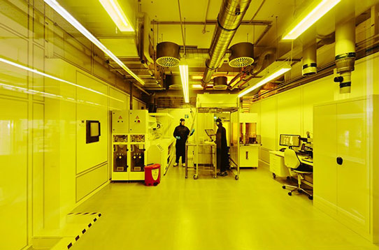
Picture: AP&S’ new Demo Center.
AP&S says that, as the purchase of a wet process application is a significant decision (in which many important aspects and complex contexts must be considered), it aims to support customers during the decision-making process to ensure they receive the optimal wet process solution that meets their specific requirements. In the new Demo Center, customers can test the wet process application of interest and obtain all crucial information, such as a comprehensive test report containing complete parameters of the process set-up, a recommendation for the process recipe due to test results, and further key system configuration details.
The firm says that the Demo Center plays a significant role not only before the booking but also during the production of the application ordered. Prior to tool delivery, the Demo Center prepares all relevant steps for rapid tool commissioning and optimal production start-up. The range of services includes an in-house process evaluation with a definition of process parameters, a calculation of the throughput and chemical consumption as well as trainings for the customer’s staff.
Available process demonstrations include: advanced metal lift-off, metal etching, mask cleaning, photoresist development and strip as well as various cleaning processes. The following wafer sizes can be handled: diameter (round substrates) up to 300mm; side length (square substrates) up to 9“; and thickness up to 10mm. Possible chuck variations are low-contact chucks, various vacuum chucks as well as back- or front-side protection chucks. Different wafer materials with various thicknesses can be processed, such as silicon, silicon carbide (SiC), gallium nitride (GaN), gallium arsenide (GaAs), sapphire, glass etc, as well as Taiko wafers (with other materials and substrate types possible).
Epitaxial lift-off Wet processing systems
www.ap-s.de/rd/demo-center.html


