


- News
6 January 2017
Multi-level metalization for high-density gallium nitride transistors on silicon
Researchers based in USA and Korea have used multi-level metalization to improve the performance and density of aluminium gallium nitride/gallium nitride (AlGaN/GaN) heterostructure field-effect transistors (HFETs) on silicon [Seung Kyu Oh et al, Appl. Phys. Express, vol10, p016502, 2017]. The devices achieved higher drain currents and a lower fall off in current at high drain bias, compared with conventional single-metal-layer HFETs of the same device area. The work involved University of Houston in the USA and Sunchon National University, Chonbuk National University and LG Electronics in Korea.
GaN-based transistors are being developed for power electronics applications with a view to replacing the present pure silicon components. The wide bandgap of GaN offers opportunities to increase carrier saturation velocities, mobility and density, along with higher critical electric field for higher breakdown voltages.
Using material grown on large-diameter silicon substrates should reduce production costs. Increasing device density should improve wafer utilization efficiency. The researchers comment: "Multi-level metalization schemes, which are well developed in the Si-based semiconductor industry, are an effective way to increase the number of dies per wafer."
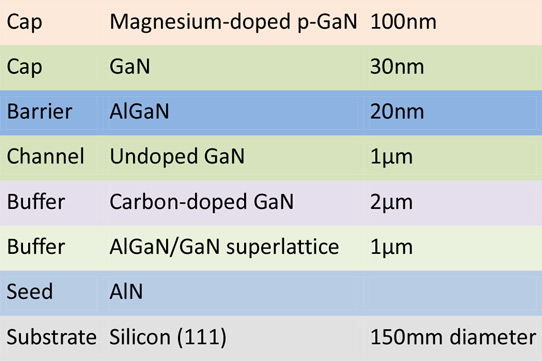
Figure 1: III-nitride heterostructure.
The III-nitride heterostructure (Figure 1) was grown on 150mm-diameter (111) silicon by metal-organic chemical vapor deposition (MOCVD). The top p-GaN layer was removed by selective inductively coupled plasma reactive-ion etch except in the gate region of the device. Further etching created device-isolation mesas. Ohmic source/drain electrodes consisted of annealed titanium/aluminium/palladium/gold (Ti/Al/Pd/Au). The gate electode was nickel/gold (Ni/Au). Plasma-enhanced chemical vapor deposition (PECVD) silicon nitride was used to passivate surface states.
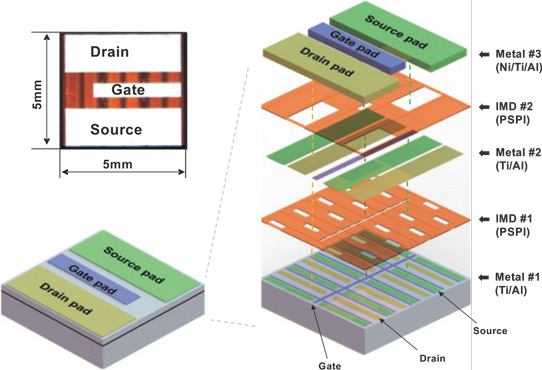
Figure 2: Schematic diagram of AlGaN/GaN HFETs with multi-level metalization.
The first metal layer consisted of Ti/Al lines, deposited after etching via holes in the silicon nitride to make contact with the devices (Figure 2). Further metal layers were separated by photosensitive polyimide (PSPI). The intermetal dielectric (IMD) was spin coated onto the wafer at 3000 rotations per minute and soft-baked at 120°C for 3 minutes. The material was patterned with via holes using mercury lamp 365nm i-line UV light and development, followed by hard-baking at 140°C for 3 minutes. Curing was carried out at 320°C for 100 minutes in nitrogen atmosphere.
The second metal layer of Ti/Al lines was deposited on the IMD with contacts through the via holes. A further layer of IMD was applied and patterned with via holes. This final IMD layer was treated with oxygen plasma to improve the adhesion between the IMD and the final Ni/Ti/Au source, gate and drain bonding pads.
The researchers comment: "In this structure, the size of the chip is significantly smaller than those of conventional devices due to the location of the bonding pad region directly on top of the active device area."
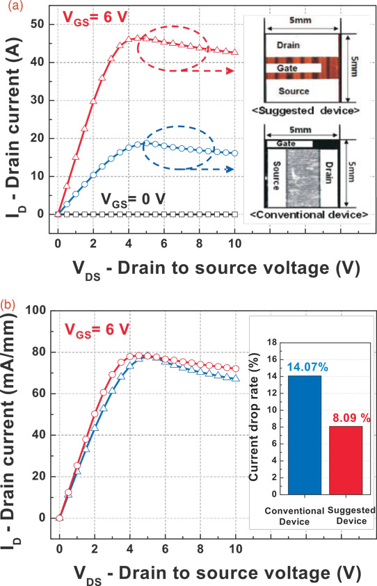
Figure 3: (a) Output power characteristics and (b) current drop ratio of AlGaN/GaN HFETs with multi-level metalization in comparison with conventional HFETs having the same chip size.
The normally-off transistors had a threshold of +0.8V. With 6V gate and 4V drain bias, the maximum drain current was 46.3A (Figure 3). With 0V gate, the current leakage was 92μA at 600V drain bias. The breakdown voltage for 500μA leakage was 635V. This was slightly lower than the 670V breakdown of a conventional HFET of the same area.
The gate width of the 5mmx5mm multi-level HFET device was 590806μm (4409μmx134), while the 5mmx5mm conventional HFET gate width was 250800μm (2200μmx114).
The maximum drain current of the conventional HFET was 18.4A with the same biasing as for the multi-level device. The researchers explain: "The maximum drain current, which is related to the output power, for the multi-level-metalization-structured HFETs is 240% higher because the multi-level metalization structure can increase the size of the active area for the same chip size."
As the drain bias increased to 10V, self-heating effects reduced the drain current with 6V gate potential 14.07% in the conventional device and 8.09% in the multi-level structure. Self-heating increases phonon scattering and hence reduces carrier mobility in the two-dimensional electron gas (2DEG) channel. The reduced drain current fall off at 10V in the multi-level HFET thus indicates improved heat dissipation. The researchers suggest that this was due to generated heat being transferred from the active area to the surface through the conductive Al via-holes.
HFETs HFETS on siliconHFETs AlGaN GaN MOCVD PECVD
https://doi.org/10.7567/APEX.10.016502
The author Mike Cooke is a freelance technology journalist who has worked in the semiconductor and advanced technology sectors since 1997.


