


- News
22 February 2017
Silicon and III-nitride high-voltage monolithic cascode diode
Hong Kong University of Science and Technology (HKUST) has developed a high-voltage monolithic cascode diode combination (Figure 1) of silicon (Si) pn diode and normally-on aluminium gallium nitride (AlGaN) barrier metal-insulator-semiconductor high-electron-mobility transistor (MIS-HEMT) [Jie Ren et al, IEEE Electron Device Letters, published online 8 February 2017].
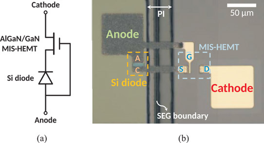
Figure 1: (a) Circuit schematic and (b) top-view image of cascoded diode.
"Compared with conventional AlGaN/GaN [Schottky barrier diodes (SBDs)], the cascoded diode can provide much lower reverse leakage current due to the superior voltage blocking capability of the MIS-HEMT and the low leakage of the Si diode," the researchers comment.
The researchers also see the monolithic integration work as leading to smaller effects from parasitic inductance, resistance, or capacitance, compared with systems assembled from a number of discrete parts. "Large parasitics will cause circuit ringing during fast switching, resulting in system instability," they add. Further potential advantages include reduced system size and production cost.
The devices were fabricated on 4-inch (111) silicon substrates (Figure 2). A 300nm layer of silicon dioxide was formed, which was etched to form a mask for the recessed window. Further etching created a 4μm-deep region for selective epitaxial growth (SEG). More silicon dioxide was deposited as a sacrificial layer that was then removed to smooth the bottom silicon surface in the recessed windows.
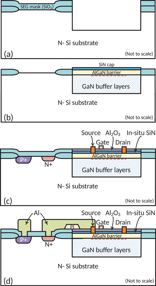
Figure 2: Schematic cross sections: (a) after recessed window formation, (b) after AlGaN/GaN epitaxial structure growth, (c) after silicon and GaN fabrication, (d) after metal-line interconnection deposition.
A new 1.5μm SiO2 SEG mask was applied before metal-organic chemical vapor deposition (MOCVD) of 280nm AlN nucleation, 1.1μm step-graded AlGaN buffer, 2.7μm GaN buffer, 100nm GaN channel, 1nm AlN spacer, 20nm Al0.3Ga0.7N barriers, and 8nm in situ silicon nitride cap.
Polycrystalline GaN on the SiO2 mask was removed with dry etching that stopped at the SiO2. Removing the SEG mask then resulted in a near-planar surface, which enabled fine-pattern lithography.
The p- and n-type regions of the silicon pn diode were formed by implantation of boron/boron difluoride (BF2) and phosphorus, respectively. Plasma-enhanced chemical vapor deposition (PECVD) was used to create a 350nm SiO2 passivation layer for the diode.
The AlGaN/GaN HEMT was fabricated by argon implantation defining the active region, selective etch of source-drain windows in the silicon nitride cap, titanium/aluminium/nickel/gold source-drain metal deposition, 830°C annealing to activate the silicon diode doping and to alloy the HEMT source-drain metal stacks, atomic layer deposition (ALD) of aluminium oxide as part of the gate insulator with the silicon nitride cap, and nickel/gold evaporation of the gate electrode.
The devices were connected using sputtered aluminium. A 2.5μm imide layer at the periphery of the SEG window improved the step coverage of the aluminium interconnect. The sputtered aluminium was also used to create the silicon pn diode contacts.
The silicon pn diode had a 50μm2 active region with a drift region 2.5μm long and 20μm wide. The active MIS-HEMT area was 190μm2 with a 2μm-long 10μm-wide gate. The gate-source and gate-drain distances were 2μm and 15μm, respectively.
The interconnect distance of 70μm reduces the parasitic inductance to around 0.03nH, compared with the ~2nH typical for conventional ~2mm wire bonding.
Individual characterization of the silicon diode gave a forward voltage of 0.8V at 500A/cm2 current density. Breakdown occurred at 22V. Meanwhile, the MIS-HEMT had an on/off current ratio of 108 and 613mA/mm drive current at 2V gate potential and 10V drain bias. The threshold voltage was -5.2V. Breakdown with 1mA/mm current density was 550V.
The cascode circuit had a turn-on voltage of 0.6V for a current density of 1A/cm2, normalized by the sum of the active areas (240μm2 = 50μm2 + 190μm2) of the component parts. At 500A/cm2, the specific on-resistance was 5.4mΩ-cm2 (differential, 2.8mΩ-cm2).
A conventional AlGaN/GaN Schottky barrier diode on the same wafer had a 0.7V turn-on and 3.7mΩ-cm2 specific on-resistance (1.8mΩ-cm2, differential). The higher on-resistance of the cascode diode is blamed on "series resistance and the additional device area needed for the silicon diode".
By contrast, the reverse bias leakage was two orders of magnitude lower for the cascode diode than for the SBD. In fact, the large reverse leakage of the SBD makes it impractical for applications, according to the researchers. In numbers, the cascode diode reverse leakage was 5.6x10⁻⁵mA/mm (1.9x10⁻⁴mA/cm2) at 300V. The 300V reverse bias is a typical bus voltage for applications using 500-600V class diodes, according to the team.
The cascode diode reverse leakage performance was "smaller than most of the state-of-the-art AlGaN/GaN SBDs," the researchers say. They attribute the small leakage to "the superior voltage-blocking capability of the MIS-HEMT and the low leakage current of the silicon diode".
The cascode diode on/off current ratio was 3x10⁶ with 1A/cm2 breakdown of 557V, which the researchers claim is 62V greater than that of the conventional AlGaN/GaN SBD.
Another area where the cascode diode improves on the AlGaN/GaN SBD is in having a low ideality factor of 1.4, compared with 2.7, indicating a sharper turn-on behavior.
Varying the temperature between 25°C and 200°C the reverse leakage of the cascode diode increased by two orders of magnitude, but this change was smaller than that of the AlGaN/GaN SBDs.
https://doi.org/10.1109/LED.2017.2665698
The author Mike Cooke is a freelance technology journalist who has worked in the semiconductor and advanced technology sectors since 1997.


