


- News
7 December 2017
University of Tokyo and Mitsubishi quantify factors for reducing SiC power semiconductor resistance by two-thirds
© Semiconductor Today Magazine / Juno Publishing
At the 63rd IEEE International Electron Devices Meeting (IEDM 2017) in San Francisco on 4 December, a university-industry team at the University of Tokyo and Mitsubishi Electric Corp in Japan reported that it has quantified for the first time the impacts of three electron-scattering mechanisms for determining the resistance of silicon carbide (SiC) power semiconductor devices in power semiconductor modules. They found that resistance under the SiC interface can be reduced by two-thirds by suppressing electron scattering by the charges. This is expected to help to reduce energy consumption in power equipment by lowering the resistance of SiC power semiconductors.
SiC power devices offer lower resistance than conventional silicon power devices, so to further lower their resistance it is important to understand correctly the characteristics of the resistance under the SiC interface.
“Until now, however, it had been difficult to measure separately resistance-limiting factors that determine electron scattering,” says Satoshi Yamakawa, senior manager of the SiC Device Development Center at Mitsubishi Electric’s Advanced Technology R&D Center.
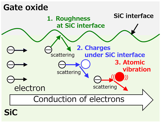
Picture: Electron scattering under the SiC interface is limited by three factors: roughness of the interface, charges under the interface, and atomic vibration.
Electron scattering focusing on atomic vibration was measured using technology from the University of Tokyo. In Mitsubishi Electric’s analyses of fabricated devices, the impact that charges and atomic vibration have on electron scattering under the SiC interface was revealed to be dominant. Although it has been recognized that electron scattering under the SiC interface is limited by three factors - namely the roughness of the SiC interface, the charges under the SiC interface, and the atomic vibration - the contribution of each factor had been unclear. A planar-type SiC metal-oxide-semiconductor field-effect transistor (SiC-MOSFET), in which electrons conduct away from the SiC interface to around several nanometers, was fabricated to confirm the impact of the charges.
“We were able to confirm at an unprecedented level that the roughness of the SiC interface has little effect while charges under the SiC interface and atomic vibration are dominant factors,” says Koji Kita, an associate professor in the University of Tokyo’s Graduate School of Engineering.
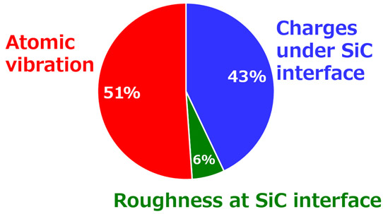
Picture: SiC interface roughness has little effect in limiting resistance, while charges under the SiC interface and atomic vibration are dominant factors.
Using an earlier planar-type SiC-MOSFET device for comparison, resistance was reduced by two-thirds due to suppression of electron scattering, which was achieved by making the electrons conduct away from the charges under the SiC interface. The previous planar-type device has the same interface structure as that of the SiC MOSFET fabricated by Mitsubishi Electric.
For the test, the firm handled the design, fabrication and analysis of the resistance-limiting factors and the University of Tokyo handled the measurement of electron-scattering factors.
“Going forward, we will continue refining the design and specifications of our SiC MOSFET to further lower the resistance of SiC power devices,” says Yamakawa.
Mitsubishi ElectricSiC power MOSFET
www.MitsubishiElectric.com/semiconductors


