


- News
14 August 2017
Controlled spalling of bulk and free-standing gallium nitride substrates
IBM T. J. Watson Research Center in the USA has been exploring controlled spalling as a method for transferring thin layers of gallium nitride (GaN) from bulk and free-standing substrates [S. W. Bedell et al, J. Appl. Phys., vol122, p025103, 2017].
The researchers see the process as potentially contributing to the application in power electronics, where at present there are difficulties in thinning GaN to increase thermal conductivity due to the material’s hardness and inertness. Also, the use of very expensive bulk and free-standing GaN substrates could be ameliorated by reusing the wafer and separating a number of device layers.
The researchers have previously reported the separation of epitaxial GaN light-emitting diode (LED) layers from sapphire substrates, along with applications of controlled spalling to silicon circuits and germanium- and gallium arsenide-based solar cells
Controlled spalling uses a tensile stressor material deposited on the surface of the GaN substrate to induce fracture inside the material that propagates across the substrate. The researchers have found nickel to be a particularly suitable stressor. The nickel can be deposited by sputtering or electro-deposition.
The substrate was 300μm-thick hydride vapor phase epitaxy (HVPE) GaN. The substrates were 2-inch diameter. The material came from various suppliers. The stressor consisted of DC magnetron sputtered layers of 90nm titanium adhesion and 1μm nickel seed for further electro-plating at room temperature. The electro-deposition used a solution containing nickel chloride (NiCl2) and boric acid (H3BO3). The nickel was applied to both sides of the substrate.
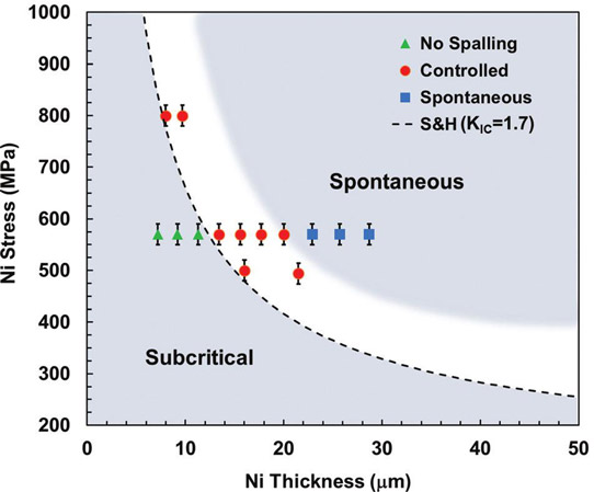
Figure 1: Plot of thickness versus stress of Ni stressor layer that defines controlled spalling regime for <0001> bulk GaN wafers.
The tensile stress in the nickel was around 450MPa to 500MPa, independent of thickness from 16μm up to 30μm (Figure 1). Adding ammonium chloride (NH3Cl) to the electro-deposition solution increased the stress to 800MPa, allowing spalling to begin at 8μm thickness.
To perform the spalling, a 25μm-thick polyimide tape was roll applied to the surface. Lifting one edge of the tape was found to initiate the fracture that could be propagated across the substrate (Figure 2).
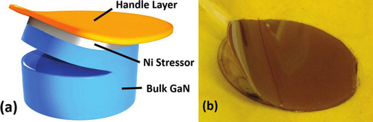
Figure 2: (a) Controlled spalling of bulk GaN substrate and (b) image of 2-inch bulk GaN wafer during process.
The researchers report: “This manual method of guiding fracture does not require any additional ‘pulling’ force on the handle layer; once the crack is initiated at the wafer edge, the mechanical energy to propagate fracture is contained in the Ni stressor layer.”
There was variation in the thickness of the spalled GaN between 18μm and 25μm, “primarily dependent on the Ni film uniformity, although local fracture perturbations can cause spalling depth variation,” the team reports.
Transmission electron microscopic (TEM) analysis gave the defect density as below the detection limit of mid 107/cm2.
One problem is that the [0001] c-planes are not natural cleavage directions in GaN. The researchers comment: “Recent work suggests that the m- and a-planes permit proper cleavage and, therefore, spalling of semi-polar and non-polar GaN wafers may have much lower as-spalled roughness.”
The researchers report: “Although we have demonstrated that controlled spalling can be used to remove thin surface films from bulk GaN substrates without generating defects or cracks in either the film or the remaining wafer, the surface artifacts presently make wafer reclaim challenging.”
The surface artifacts were seen when the spalling process was started and stopped. The artifacts presented as depth perturbations of order 1-2μm. The team suggests that improvement in the technique for wafer reclaim would require constant velocity fracture propagation or new higher-speed grinding and lapping.
Double-side-polished GaN wafers allowed spalling from the N-face. The researchers found no difference in spalling characteristics between Ga- and N-faces.
GaN Free-standing GaN substrates HVPE
http://dx.doi.org/10.1063/1.4986646
The author Mike Cooke is a freelance technology journalist who has worked in the semiconductor and advanced technology sectors since 1997.


