


- News
2 September 2016
Boosting transconductance in indium gallium arsenide finFETs
Researchers at Massachusetts Institute of Technology (MIT) in the USA have claimed record transconductance for III-V fin field-effect transistors (finFETs) when normalized according to fin width [Alon Vardi and Jesús A. del Alamo, IEEE Electron Device Letters, 1 August 2016]. Up to now, indium gallium arsenide (InGaAs) finFETs III-V have delivered disappointing results, particularly with very narrow fins.
Vardi and del Alamo report: "Our fabrication process closely follows CMOS requirements, particularly self-alignment of refractory gate and ohmic contacts, very low thermal budget, extensive use of [reactive ion etch] RIE and an entirely lift-off free process in the front end." The only lift-off step is a final back-end step for via opening and pad formation.
The researchers used a contact-first, gate-last approach that has given record transconductance in InGaAs quantum well metal-oxide-semiconductor field-effect transistors (MOSFETs). The channel material consisted of a 40nm In0.53Ga0.47As layer in the heterostructure. The contacts consisted of molybdenum/tungsten.
The gate region was defined using silicon dioxide and molybdenum. The fins were etched with reactive ion etch, followed by a more exact digital etch process of several cycles, smoothing and trimming the sidewalls. Within 5 minutes of the fin etch, the gate region was coated with high-k dielectric by atomic layer deposition (ALD) and then the molybdenum gate metal was sputtered and etched.
Devices consisted of 10-50 parallel fins with fin-pitch 200nm. The finFETs were actually double-gate rather than triple-gate devices, since the hydrogen silsesquioxane (HSQ) photoresist used to define the fin etch was not removed during gate formation.
Vardi and del Alamo comment: "While theoretically inferior to tri-gate designs, practically, the greater simplicity of the process allows us to aggressively scale all device dimensions and implement a self-aligned process. This ultimately results in significantly better performance than prior InGaAs tri-gate MOSFET demonstrations." They also point out that with thinner fins the top gate offers diminishing returns in performance.
A device with 30nm gate length and 7nm fin width (Figure 1) achieved a peak transconductance of 900μS/μm and on-resistance of 320Ω- μm with 0.5V drain bias. The normalization is according to the standard conducting periphery – in this case the two gates per fin give 2x the channel height. The saturated subthreshold swing was 100mV/decade; the drain-induced barrier lowering was 90mV/V at 0.5V.
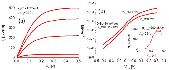
Figure 1. (a) Output and (b) subthreshold characteristics of InGaAs finFET with 7nm fin width, 30nm gate length. Inset: transconductance (gm) characteristics.
Increasing the fin width to 22nm increased the peak transconductance to 1500μS/μm. With 22nm-wide fins and 2μm gate length, the linear subthreshold swing reduced to as low as 68mV/decade, close to the theoretical minimum for planar devices of 60mV/decade at room temperature. The low swing is taken as indicating a high-quality semiconductor sidewall/gate dielectric interface.
In a range of devices with varying gate length and equivalent oxide thickness (EOT) of the high-k dielectric, Vardi and del Alamo found "classic finFET scaling behavior that has not experimentally been demonstrated before with InGaAs". In particular, transconductance increased with reduced gate length, while EOT reduction gave increased transconductance, threshold voltage roll-off mitigation, and enhancement of saturated subthreshold swing.
On the other hand, reducing fin width resulted in degraded transconductance. Vardi and del Alamo suggest this may be due to sidewall roughness leading to increased carrier scattering. Thinner fin widths, however, do lead to higher threshold voltages, although this is partly due to mobility degradation. Quantum effects are another possible contributing factor.
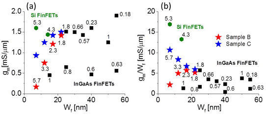
Figure 2. Benchmark of maximum gm versus fin width (Wf) for InGaAs finFETs and state-of-the-art silicon finFETs. On the left, gm is normalized by gate periphery. On the right, gm is normalized by fin footprint. Numbers next to each data point represent the aspect ratio of the conducting channel.
In benchmarking their transconductance results against other reports, including silicon-based finFETs, Vardi and del Alamo use two normalizations (Figure 2). Using the standard gate periphery normalization, silicon and InGaAs devices seem to have comparable performance. However, basing the normalization on fin width is more relevant for transistor density and the benchmarking shows a gap between Si and InGaAs. "This stems from the high aspect ratio of Si fins and reveals the significantly greater effectiveness in charge control modulation through the sidewalls in Si finFETs when contrasted with InGaAs finFETs," Vardi and del Alamo write. However, their new InGaAs finFETs show a factor of nearly two improvement in performance over previous reports, closing the gap with silicon.
http://ieeexplore.ieee.org/xpl/articleDetails.jsp?arnumber=7527654
The author Mike Cooke is a freelance technology journalist who has worked in the semiconductor and advanced technology sectors since 1997.


