


- News
14 October 2016
Combatting droop with thick single quantum wells on semi-polar GaN
University of California Santa Barbara (UCSB) has used thicker single quantum wells (SQWs) of indium gallium nitride (InGaN) on free-standing semi-polar gallium nitride to create a light-emitting diode (LED) with 'negligible' external quantum efficiency (EQE) droop up to 900mA injection current and almost 1W output power [Sang Ho Oh et al, Appl. Phys. Express, vol9, p102102, 2016].
The researchers comment: "The adoption of a thick active region resulted in excellent optical and thermal performance characteristics that are suitable for high-power lighting applications."
Previous attempts to use thicker SQWs on c-plane templates have resulted in low performance due to poor overlap between the electrons and holes that should recombine into photons. The poor overlap is related to large electrical fields in the c-direction arising from charge polarization of the III-nitride bond. Net electric fields tend to pull the electrons and holes apart, reducing radiative recombination into photons.
Narrower wells on c-plane help confine the electron and hole wavefunctions, increasing overlap. Multiple quantum wells are often used in an attempt to increase brightness, but this is not terribly successful since holes tend to only be injected into the well nearest to the p-contact layers.
The use of semi-polar material increases radiative recombination by increasing the overlap without the need for confinement. The diode built-in electric field approximately cancels the reduced field arising from charge polarization effects in (20-2-1) semi-polar oriented material.
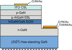
Figure 1: Schematic of 1mm2 (20-2-1) LED with roughened back side.
The UCSB LED material (Figure 1) was grown on 5mmx10mm pieces of (20-2-1) GaN by metal-organic chemical vapor deposition (MOCVD). The free-standing substrate was supplied by Mitsubishi Chemical.
The active SQW region consisted of a 9nm GaN barrier, 14nm or 12nm In0.16Ga0.84N, and a 16nm GaN barrier. The n-GaN contact layer was 1μm thick. The p-type layers included a 15nm aluminium gallium nitride (AlGaN) electron-blocking layer (EBL). The p-GaN contact layer was 115nm.
The material was fabricated into 1mm2-mesa LEDs with 220nm indium tin oxide (ITO) current-spreading layer (CSL) on the p-contact, annealed titanium/aluminium/nickel/gold n-electrode, and chromium/nickel/gold n- and p-contact pads. The back-side of the device was plasma etched to improve light extraction.
The 14nm SQW device was package in a vertical transparent stand process. The submount was zinc oxide. The assembly was encapsulated in transparent silicone with 1.41 refractive index. The 12nm SQW LED was mounted on a heating stage without encapsulation.
Table 1: Output power and EQE at different current injection levels for (20-2-1) blue LED with 14nm SQW.
| Current | Output power | EQE |
| 100mA | 112mW | 40.1% |
| 200mA | 236mW | 42.3% |
| 500mA | 574mW | 41.1% |
| 900mA | 991mW | 39.4% |
The output power and external quantum efficiency of the 14nm SQW LED showed much improved performance with respect to current (Table 1). The peak EQE of 42.3% occurred at 200mA. The peak EQE was only slightly lower than for a previous smaller-area (0.1mm2) device. The difference is explained as being due to reduced light-extraction efficiency and current-crowding effects of larger-area LEDs. However, at 900mA current injection the device shows 'negligible' efficiency droop, which the researchers attribute to the lower carrier density allowed by the thick SQW.
While the EQE (photons/electron) is approximately flat above the peak, the wall-plug efficiency (WPE, output/input power) declines due to an increase in forward voltage. The researchers comment: "The forward voltage at 200mA (20A/cm2) is 3.6V, which is relatively high compared with those of commercial LEDs, and results in a reduction in WPE at drive currents. Further optimization of the resistance of the p-contacts, n-contacts, ITO current-spreading layers, and n-GaN current-spreading layers should reduce the forward voltage and increase the WPE of the LEDs."
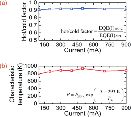
Figure 2: (a) Dependence of hot/cold factor on current for (20-2-1) blue LED with 12nm SQW. (b) Dependence of characteristic temperature on current for same LED (T = 100°C).
The 12nm SQW LED was used in temperature characterization. The demonstrated EQE was less than 15%. This was due to the horizontal orientation and absence of encapsulation, according to the team. Increasing the temperature reduced the EQE, but did not add any efficiency droop, which was small at all temperatures up to 100°C. The hot/cold factor of EQE at 100°C/20°C was constant at around 0.9 for currents between 100mA and 900mA (0.92 factor). The characteristic temperature for the output power droop was more than 800K (884K at 900mA).
The researchers maintain that these results indicate thermionic escape had an insignificant effect on droop. "This indicates that carrier leakage due to the thermionic escape is unlikely to be a cause of the efficiency droop," they add.
The researchers also found that the temperature dependence was similar to that of small-area 0.1mm2 devices. They conclude that the new devices are "well suited for high-power solid-state lighting applications that require thermal stability".
UCSB SQWs InGaN Free standing semi polar GaN LEDs
http://doi.org/10.7567/APEX.9.102102
The author Mike Cooke is a freelance technology journalist who has worked in the semiconductor and advanced technology sectors since 1997.


