


- News
16 November 2016
Three-prong attack to improve quaternary solar cell MBE
Researchers based in USA and Spain say they have doubled the AM1.5G conversion efficiency of ~2.0eV aluminium indium gallium phosphide (AlGaInP) solar cells grown by molecular beam epitaxy (MBE) compared with previous work [J. Faucher et al, Appl. Phys. Lett., vol109, p172105, 2016].
The team from Yale University in the USA, Universidad Rey Juan Carlos in Spain, and University of Illinois at Urbana-Champaign in the USA see applications in multi-junction devices for high-efficiency space vehicle power and concentrator photovoltaics. Combined in 5-6 junction structures it is hoped that conversion efficiencies greater than 50% could be achieved. Existing 3-4 junction devices with more than 44% efficiency seem to be reaching the limit for such designs.
The team used three approaches to improve performance: the introduction of AlGaInP-AlInP grading near the window and back surface field (BSF) regions; optimization of the growth process and device design; and post-growth annealing.
Aluminium-containing solar cell layers suffer from oxygen-related defects, sapping performance. AlGaInP devices grown by MBE have previously had poor performance compared with material grown by organometallic vapor phase epitaxy (OMVPE). The researchers have managed to improve the performance of MBE-grown structures to a level comparable to OMVPE.
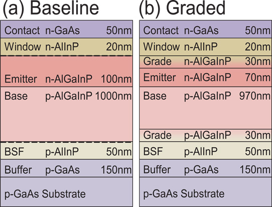
Figure 1: Layer structures for (a) baseline AlGaInP solar cells with abrupt heterojunctions denoted by black dashed lines and (b) cells with AlGaInP compositionally graded heterojunctions.
The MBE (Figure 1) was performed on gallium arsenide (GaAs) to give cells responsive to photons of ~2.0eV energy. The AlGaInP and AlInP layers were initially grown at 460°C. The AlInP had 50% Al content and the AlGaInP 10% Al. Two structures were produced: one with sharp transitions between the different Al composition (comparison baseline), and the other graded.
Compositional grading was achieved by varying the Al and Ga fluxes, seeking to provide a monotonic change in bandgap and minimal lattice mismatch. The researchers also hoped that by avoiding pauses between AlGaInP and AlInP the incorporation of oxygen and other trap states in the transition region would be reduced. Transmission electron microscopy (TEM) did not show any dislocations in the transition region. However, high-angle annular dark field images did show slight phase separation of the cell ternary and quaternary materials. The team comments that this is common for such alloys grown by MBE.
The internal quantum efficiency peak of the graded structure was measured at 74%. The bandgap-voltage offset – the difference between the bandgap-voltage and open-circuit voltages (WOC = Eg/q – VOC) – was 616mV. The IQE of the baseline structure peaked around 60%. The bandgap-voltage offset was the same as for the graded structure.
Further optimization of the growth process involved varying growth rates, V/III ratios, and substrate temperature with a view to increasing carrier diffusion lengths. With 490°C temperature the electron diffusion length was doubled to around 910nm, according to simulations. At the same time, peak IQE increased to 80% and WOC was reduced to 602mV. The performance was relatively insensitive to growth rate and V/III ratio variations.
Short-circuit current (Jsc) was increased by 1.16x by reducing photon absorption in the upper layers through decreasing the combined grade and emitter thickness to 70nm. At the same time, WOC was further reduced to 573mV. The base layer was increased to 1.5μm to reduce transmission losses.
The researchers suggest that changing the n-type silicon doping to selenium might further improve performance. In OMVPE, such a change has led to improvements in IQE, short-circuit current, and open-circuit voltage.
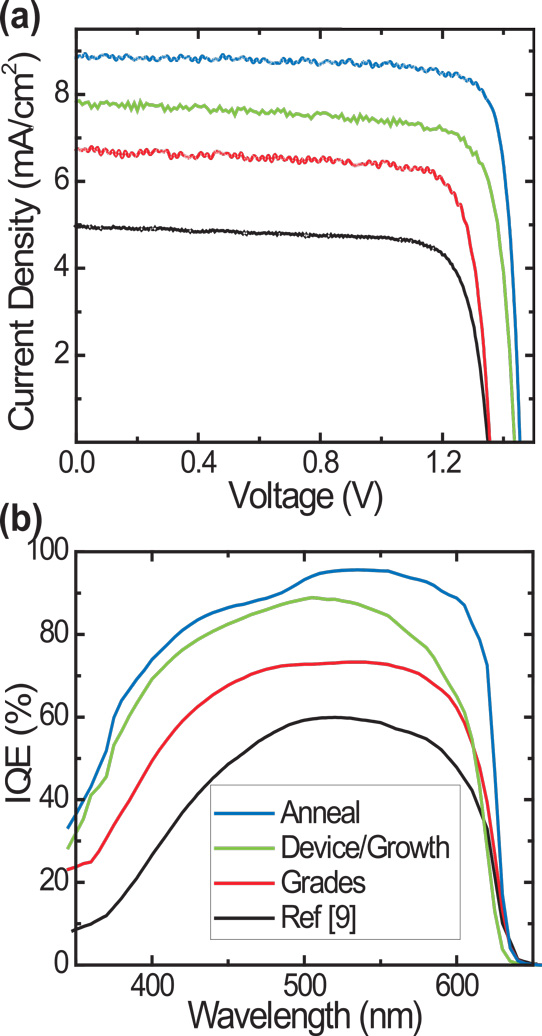
Figure 2: (a) Current–voltage characteristics under AM1.5G illumination and (b) IQE showing improvements over previously reported MBE-grown AlGaInP cells (black) by incorporating AlGaInP grades (red), growth window and device structure optimization (green), and post-growth annealing (blue).
A final strategy to improve performance was an anneal immediately after the MBE growth. A 670°C 5-minute thermal process reduced dark current by a factor of about 4 (Figure 2). The researchers estimate the electron diffusion length to be more than 2000nm. The IQE peak increased to 95%. Short-circuit current also increased to 9.0mA/cm2. The bandgap-voltage offset was 520mV.
The team comments: "Most of the Jsc increase with annealing arises from improvements in long-wavelength IQE, implying significantly improved material quality in the p-type base."
The fill-factor increased to ~0.85, giving a conversion efficiency of 10.9%.
AlGaInP solar cells AlGaInP Solar cells MBE
http://dx.doi.org/10.1063/1.4965979
The author Mike Cooke is a freelance technology journalist who has worked in the semiconductor and advanced technology sectors since 1997.


