


- News
25 May 2016
Monolithic quantum dot infrared photodetectors on silicon
Researchers based in the UK, USA and Germany claim the first direct growth of mid-infrared indium arsenide in gallium arsenide (InAs/GaAs) quantum dot infrared photodetectors (QDIPs) on silicon substrates by molecular beam epitaxy [Jiang Wu et al, ACS Photonics, vol3, p749, 2016]. The team is at University College London in the UK, University of Arkansas in the USA, Humboldt University in Berlin, Germany, and the United States Army Research Laboratory.
The direct growth of GaAs on silicon is hampered by lattice (~4%) and thermal expansion coefficient (TEC) mismatches, which generate dislocations.
The researchers believe that direct growth of infrared photodetectors on silicon could lead the way to high-performance, multispectral and large-format infrared focal plane arrays (FPAs) for hyperspectral imaging, infrared spectroscopy, and target identification. This would be based on monolithic integration of photodetector structures with silicon-based readout electronics.
Other possible uses of such detectors include free-space communication, surveillance, tracking and missile interception, chemical sensing, and biomedical imaging.
Of course, there exist technologies for such applications, but these tend to be expensive and difficult to fabricate, such as devices based on mercury cadmium telluride (MCT) semiconductors. In particular, readout circuitry is processed separately from the photodetector, before hybrid assembly into focal plane arrays.
Monolithic integration should lead to faster speed, higher performance, enhanced functionality, higher resolution, and reduced fabrication costs.
The team grew III-V material on silicon substrate by solid-source molecular beam epitaxy (SS-MBE). Antiphase domains were avoided by growth on (100) substrates offcut 4° in the [011] direction. After a 5nm aluminium arsenide nucleation layer, the researchers grew a series of five GaAs buffer layers separated by four InGaAs/GaAs strained layer superlattice (SLS) threading dislocation filters (Figure 1). Without a dislocation filter, 1μm GaAs buffers exhibited a dislocation density of 109/cm2. This was reduced to 106/cm2 with the superlattices.
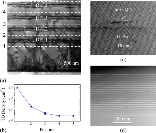
Figure 1: (a) Bright-field multi-beam transmission electron microscope (TEM) image showing threading dislocation reduction induced by dislocation filter layers. (b) Estimated threading dislocations from TEM measurements at different positions in GaAs buffer, as indicated in (a). (c) Representative high-resolution TEM image of single InAs/GaAs QD. (d) Low-magnification bright-field scanning TEM images of 20 layers of QDs.
The QDIP structure consisted of a 500nm n-GaAs contact, 80nm GaAs spacer, a sequence of 20 quantum dot layers separated by 50nm GaAs spacers, a 80nm GaAs spacer, and a 300nm top n-GaAs contact. The InAs dots were formed from a 2.1 monolayer of InAs that coalesced into discs of about 25nm diameter and 5nm height. Photoluminescence (PL) analysis suggested that the dot sizes were quite inhomogeneous.
Studying thermal quenching in the PL above 200K, the researchers estimate an activation energy of 226±27.3eV, which is roughly the difference in energy between the dots' ground state and the GaAs conduction band.
Measurements of the decay of the PL at 10K gave a long lifetime of ~1.3 nanoseconds, comparable to the performance of InAs quantum dots on GaAs substrate. The researchers comment: "The long decay-time signals that the dominant PL decay for the QD states is radiative recombination. Therefore, the long-lived PL in the QDs suggests the GaAs buffer technique used here provides a high-quality QDIP with low defect density."
Mesa QDIPs were fabricated with annealed nickel/germanium-gold/nickel/gold top and bottom contacts. The 1V dark current was "rather low", according to the researchers: 8.9x10⁻⁴A/cm2 at 60K and 2.8x10⁻³A/cm2 at 80K (Figure 2). The mesa was 1mm in diameter. The researchers comment: "Despite the presence of threading dislocations (∼106/cm2) caused by the large lattice and TEC mismatch, the QDIP on Si shows comparable dark current density to state-of-the-art devices grown on a native substrate."
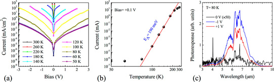
Figure 2: (a) Dark current-voltage characteristics at different temperatures for InAs/GaAs QDIP. (b) Dark-current activation energy extracted from dark current measured under 0.1V bias. Fitting error is 1.9meV. (c) Photocurrent spectra measured with different bias voltages at 80K.
The team also points out that its device does not use a current-blocking layer to reduce dark current. The dark current activation energy was 190±1.9meV, slightly lower than the photoluminescence thermal quenching value. The hole activation energy is therefore estimated at ~36meV.
The main peak of the photo-response was located at 6.5μm wavelength, 190.7meV energy, agreeing with the dark-current activation energy. The researchers say that this supports a mechanism of bound-to-continuum transitions. The peak was broad with a full-width at half maximum (FWHM) of 2.0μm.
Mid-infrared InAs GaAs quantum dot infrared photodetectors InAs/GaAs Silicon substrates MBE
http://pubs.acs.org/doi/abs/10.1021/acsphotonics.6b00076
The author Mike Cooke is a freelance technology journalist who has worked in the semiconductor and advanced technology sectors since 1997.


