


- News
18 May 2016
More indium gallium nitride integrated photonics on silicon
Researchers in China have reported further work on integrating III-nitride devices with III-nitride waveguides on silicon [Yongjin Wang et al, Appl. Phys. Lett., vol108, p162102, 2016]. The team from University of Posts and Telecommunications and Nanjing Institute of Technology has also recently published a report of two diode devices linked by a waveguide.
The diodes can be operated either as light-emitting diodes (LEDs) or as photodiodes/detectors. By combining the output and input modes, the researchers foresee "diverse applications, opening the way to develop sophisticated integrated photonic circuits in the visible wavelength region."
The large difference in refractive index between gallium nitride (~2.45) and air (1) leads to total internal reflection, which makes it difficult to extract light from LEDs. However, total internal reflection is just what is needed for efficient low-loss confinement in waveguides.
The researchers used 2-inch III-nitride-on-silicon epitaxial wafers with a 900nm aluminium gallium nitride (AlGaN) buffer, 400nm of GaN, 3.2μm n-GaN, 250nm multiple indium gallium nitride (InGaN) quantum wells (MQWs) in GaN barriers, and 220nm of p-GaN.
The fabrication process (Figure 1) consisted of inductively coupled plasma reactive ion etching (ICP-RIE) of mesas, nickel/gold contact deposition, 500°C annealing, further ICP-RIE to give multiple waveguides, deep reactive ion etch (DRIE) of the silicon substrate under the device region, and final etching of III-nitride material to give 3μm-thick suspended membranes. Before the backside etching the top layers were protected with 6.7μm-thick photoresist.
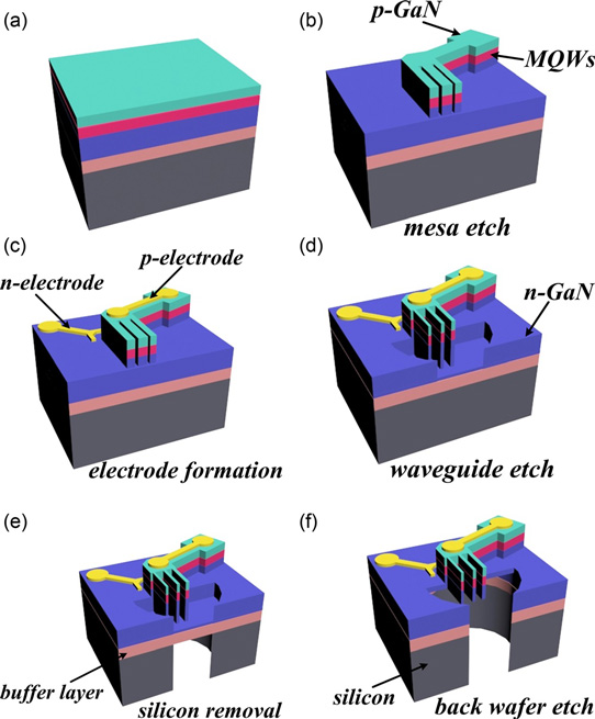
Figure 1: Schematic fabrication process of on-chip integration of suspended pn-junction InGaN/GaN MQW device and multiple waveguides.
The resulting structures were somewhat deformed due to stress release after removal of the silicon. Three 50μm-long waveguides were produced with different thicknesses: 12μm, 10μm and 8μm. The height was given by the 3μm membrane thickness.
The device was wire bonded to a test pad for characterization. As an LED, the device emitted blue light with 449.2nm dominant wavelength at 4V bias. There were also two sub-peaks at 467.5nm and 494.1nm (blue-green).
In-plane data transmission from the LEDs driven by an arbitrary waveform generator showed good performance from the 12μm-wide waveguide up to 25 megabits per second (Mbps) with open eye diagrams indicating low signal distortion (Figure 2). Narrower waveguides restrict the occurrence of multi-mode transmission. Since multi-mode transmission leads to pulse broadening due to the different transmission velocities, narrow waveguides should have higher transmission rates.
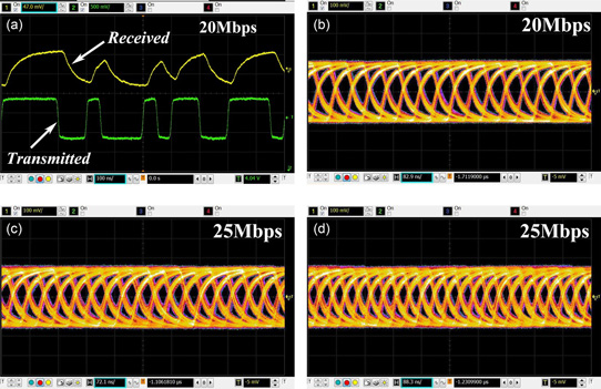
Figure 2: (a) Received output signal for 12μm-wide suspended waveguide; (b) eye diagram at 20Mbps for 12μm-wide suspended waveguide; (c) eye diagram at 25Mbps for 12μm-wide suspended waveguide; and (d) eye diagram at 25Mbps for 8μm-wide suspended waveguide.
Reversing the light direction, so that the device operated as a photodiode, 450nm light from an optical fiber was focused on the waveguide facets. With a mechanical shutter giving 0.2 seconds on and 0.2 seconds off, -42nA photocurrent at 0V bias was observed with 70μW input power on the 10μm waveguide.
InGaN integrated photonics on silicon InGaN LEDs
http://dx.doi.org/10.1063/1.4947280
The author Mike Cooke is a freelance technology journalist who has worked in the semiconductor and advanced technology sectors since 1997.


