


- News
16 May 2016
IQE joins imec's GaN-on-Si Industrial Affiliation Program
Epiwafer foundry and substrate maker IQE plc of Cardiff, Wales, UK has announced a strategic partnership on gallium nitride-on-silicon (GaN-on-Si) technology with nanoelectronics research centre imec of Leuven, Belgium.
GaN technology offers faster power-switching devices with higher breakdown voltage and lower on-resistance than silicon, suiting advanced power electronic components. The partnership builds on promising results achieved in a recent project, in which imec and IQE collaborated to fabricate GaN power diodes using imec's proprietary diode architecture and IQE's high-voltage epiwafers.
imec's GaN-on-Si Industrial Affiliation Program offers joint R&D on GaN-on-Si 200mm epitaxy and enhancement-mode device technology to companies including integrated device manufacturers (IDMs), equipment and material suppliers, fabless design houses and packaging companies. The program includes research on novel substrates to improve the quality of epitaxial layers, new isolation modules to enhance integration levels, and advanced vertical device development. As a GaN-on-Si Program partner, IQE gains access to next-generation epitaxy, devices and power electronics processes, including imec's complete 200mm CMOS-compatible GaN process line.
"The importance of GaN-on-Si for power devices cannot be understated, particularly as we enter an era of electrically propelled transportation and increasing demands for energy-efficient power control systems that require high-voltage and high-power capabilities," says Wayne Johnson, head of IQE's Power business unit. "IQE's proven track record in developing and manufacturing GaN-based epiwafers, coupled with imec's unquestionable reputation for world-leading research in nanoelectronics, makes for a powerful collaboration in this rapidly growing technology space," he adds.
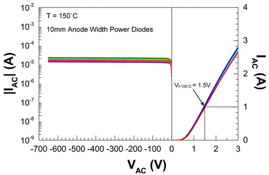
Picture: Forward and reverse diode current at high temperature (150◦C). The diodes have 10mm anode width and an anode-to-cathode distance of 10µm.
In its earlier collaborative project, imec worked with IQE to create state-of-the-art GaN power diodes. Imec has applied its proprietary gated edge terminated (GET) Schottky diode device architecture to IQE's high-voltage GaN buffers on 200mm silicon substrates. The main challenge on power diodes is to obtain devices that simultaneously show low leakage current and low turn-on voltage. Due to the GET diode device architecture and to the low buffer leakage current of IQE wafers, the large GaN power diodes (10mm), which were fabricated in imec's 200mm silicon pilot line, showed a low leakage current (up to 650V) and low turn-on voltage. The power Schottky diodes reaches forward and reverse specifications across the full temperature range, spanning from 25˚C to 150˚C with a tight distribution.
"Our joint results show that the IQE epiwafers are of excellent quality and are well aligned to meet the specifications for power Schottky diodes," comments Rudi Cartuyvels, executive VP smart systems and energy technology at imec. We look forward to collaborating with IQE to advance our promising results, which demonstrate that our proprietary GET Schottky diode device architecture and process technology can be transferred to external wafers like those provided by IQE," he adds. "Our 200mm GaN-on-Si process is available to our program partners and is engineered to fit partner specific product needs."
Imec extends GaN-on-Si R&D initiative for joint research on 200mm epi and E-mode device


