


- News
19 February 2016
Imec and VUB claim first tunable balance network for electrical balance duplexers supporting all 0.7-1GHz LTE bands
At the 2016 IEEE International Solid-State Circuits Conference (ISSCC) in San Francisco at the beginning of February, nanoelectronics research center imec of Leuven, Belgium and Vrije Universiteit Brussel (VUB) presented a frequency-division duplex (FDD) balance network - fabricated in 0.18µm partially depleted RF silicon-on-insulator (SOI) CMOS technology - capable of dual-frequency impedance tuning for all LTE bands in the 0.7-1GHz range. When integrated into an electrical-balance duplexer (EBD), it enables FDD duplexing with antennas in real-world environments, paving the way to high-performance, low-power, low-cost solutions for mobile communication.
An electrical balance duplexer is a tunable RF front-end concept that seeks to address several key challenges of 4G and 5G mobile systems. It balances an on-chip tunable impedance (the balance network) with the antenna impedance, to provide transmit-to-receive (TX-to-RX) isolation and avoid unwanted frequency components in the received signal. It is said to be a promising alternative to the fixed-frequency surface acoustic wave (SAW) filters implemented in existing mobile phones, as more and more SAW duplexers would be needed to support the ever growing amount of bands adopted by operators, increasing the size and cost of these devices. Unlike filter-based front-ends, electrical-balance duplexers provide signal cancellation, which could help to enable in-band full-duplex for double capacity and increased network density (among other benefits) for next-generation standards.
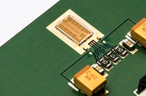 Picture: The tunable balance network chip.
Imec and VUB claim that the dual-frequency balance network is the first FDD balance network that allows balancing the on-chip tunable impedance profile with the impedance profile of an antenna at two frequencies, simultaneously. This is crucial because in real-world situations the frequency-dependent impedance of an antenna varies over environmental conditions and limits the achievable isolation bandwidth. The balance network can generate, for any LTE band within 0.7-1GHz, a simultaneous transmit-frequency impedance and receive-frequency impedance to provide high TX-to-RX isolation at both frequencies. The 0.18µm partially depleted RF SOI CMOS technology allows the balance network to better withstand the large voltages present in the EBD during full-power TX operation. The active area of the balance network (which consists of 19 switched capacitors and 10 inductors) is 8.28mm2. It is tuned by an in-house-developed custom algorithm, which can optimize the tuning codes of all 19 capacitor banks using only the isolation at the TX and RX frequencies as input.


