


- News
29 April 2016
Aluminium gallium nitride nanowire UV LED fabricated on metal foil
Ohio State University in the USA has produced aluminium gallium nitride (AlGaN) nanowire ultraviolet (UV) light-emitting diodes (LEDs) on flexible metal foil [Brelon J. May et al, Appl. Phys. Lett., vol108, p141103, 2016]. The researchers comment: "The realization of operational nanoLEDs grown directly on flexible metal foils provides a first step towards scalable roll-to-roll manufacturing of nanomaterial based solid-state optoelectronics."
Due to the confined attachment of nanowires to substrates, lattice mismatching is less important than for normal III-nitride heterostructures with planar films. Large lattice mismatch can be accommodated in nanowire heterostructures without generating dislocations.
Advantages of growing nanowires on flexible metal foils include lower costs, thermal management, and increased light extraction in top-emitting devices. Demonstrations have already been carried out on metal films on rigid substrate. Successful development of processes on flexible foils opens up the possibility of very-large-scale roll-to-roll manufacturing.
The nanowires were grown on titanium (Ti) and tantalum (Ta) metal foils through molecular beam epitaxy (MBE). The researchers believe that a wider variety of metal foils compatible with the growth temperatures could be used.
The 1-inch-square Ta and Ti foil substrates were 99.9% and 99.6% pure, respectively. The GaN nanowires were grown with a III/V ratio of 0.18. The substrates were rotated away from the nitrogen plasma source to avoid nitridation. A two-step MBE process was used with nucleation at 750°C for 5 minutes and main growth at 800°C for two hours. The same process was also used to grow GaN nanowires on silicon.
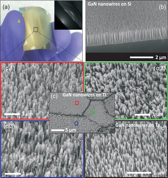
Figure 1: (a) GaN nanowires on flexible Ti foil (the inset shows a reflection high-energy electron diffraction (RHEED) pattern of nanowires on Ti foil) and scanning electron microscope (SEM) images of GaN nanowires on (b) silicon single-crystal (111) substrate, (c) different grains in the Ti foil, and (d) Ta foil.
The nanowires grew approximately perpendicular to the silicon substrates along the c-axis of the GaN crystal structure (Figure 1). The nanowires on foil were tilted according to the crystal grain structure of the metals. The grains also affected the density of nanowires.
The researchers report: "The Ta foil gives less variation between regions, and the individual regions are larger than those compared to the Ti foil."
The nanowire heights and diameters were similar on the different substrates.
Micro-photoluminescence studies at 27.6K showed a dominant peak from neutral-donor-bound exciton (D0, XA) recombination (~358nm, ~3.472eV). There was also a shoulder on the short-wavelength side of the peak from free excitons (XA, ~357.5nm, ~3.477eV). A broad peak around 362.7nm, 3.427eV, was also observed, most strongly on Ta (~0.45 main peak height) and weakly on Ti and Si (both ~0.1, shoulder-like).
The broad peak has been seen before in nanowires and possible explanations include surface-related excitons, excitons bound to structural defects, or emission from defects near the bottom surface of the nanowires.
Poor-quality GaN can give rise to yellow luminescence from defects, but this was not seen in the any of the nanowire samples.
Time-resolved photoluminescence also showed that the nanowires on Ta have similar behavior to those on Si. The nanowires on Ti had reduced emission on short time-scales and enhanced emission on longer time-scales. "Even with this variation, the relatively similar recombination characteristics for all the samples indicate that the nanowires grown on metal foils are of similar optical quality to those grown on single-crystalline Si substrates," the researchers comment.
AlGaN nanowire LEDs with integrated tunnel junction were produced on Ta foil. The heterostructure design followed previous work on silicon: 750°C n-GaN nucleation, 100nm 790°C n-GaN, polarization-engineered indium gallium nitride tunnel junction, polarization-doped p-AlGaN graded from GaN to AlN, 840°C 3-period AlGaN quantum wells in AlN barriers, and finally an AlN to GaN graded n-contact.
The LED fabrication consisted of hydrochloric acid etch to remove surface oxides from the nanowires and deposition of titanium/gold semi-transparent metal top contact. The bottom contact was fabricated by mechanically removing nanowires and diffusing an indium dot on the Ta foil.
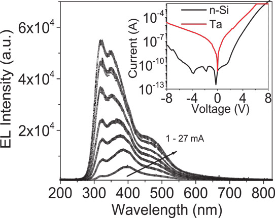
Figure 2: Electroluminescence measurements of nanowire LEDs grown directly on flexible Ta foil; the inset shows current-voltage characteristics of LED on Ta (red) compared to similar device on Si (black).
The resulting LED emitted ultraviolet light around 350nm wavelength (Figure 2). The turn-on voltage was around 5V, similar to devices fabricated on n-type silicon. Charge-polarization effects were seen in a quantum-confined Stark effect (QCSE) blue-shift at higher currents.
The intensity of the electroluminscence (EL) was a factor of 16 lower than in devices on n-Si. The team comments: "This is likely from the inhomogeneous distribution in nanowire tilt and density. Such variations could result in metal deposition on the sidewalls of the nanowires and substrate during fabrication of the top contact. Consequently, a leakage pathway is formed, reducing the number of active nanowires, thus decreasing the overall EL intensity."
The researchers hope to improve performance through optimizing the growth conditions for more uniform nanowire density and planarization.
AlGaN nanowire UV LED AlGaN UV LED Metal foil MBE
http://dx.doi.org/10.1063/1.4945419
The author Mike Cooke is a freelance technology journalist who has worked in the semiconductor and advanced technology sectors since 1997.


