


- News
14 October 2015
Alternating current light-emitting diodes on silicon
Canada's McGill University has claimed the first demonstration of alternating current (AC) III-nitride nanowire light-emitting diodes (LEDs) on silicon enabled by tunnel junctions [S. M. Sadaf et al, Nano Letters published online, 18 September 2015]. The tunnel junction connections also allow stacking of active regions of different wavelength to give white light emission without phosphors.
The researchers comment: "In general, stacking multiple quantum wells/dots in planar structures is not a suitable route to realize low-current, high-voltage operation since it also significantly increases the densities of defects and dislocations. Such issues can be fundamentally addressed in tunnel junction nanowire LED structures, as demonstrated in this work."
The N-polar nanowires (Figure 1) were grown on n-type (111) silicon using radio frequency plasma-assisted molecular beam epitaxy (PAMBE). The active regions consisted of indium gallium nitride (InGaN) self-organized quantum dots (QDs) in GaN. The self-organization was strain-induced. The dot height was ~3nm. The QD layers were capped with 3nm of GaN.
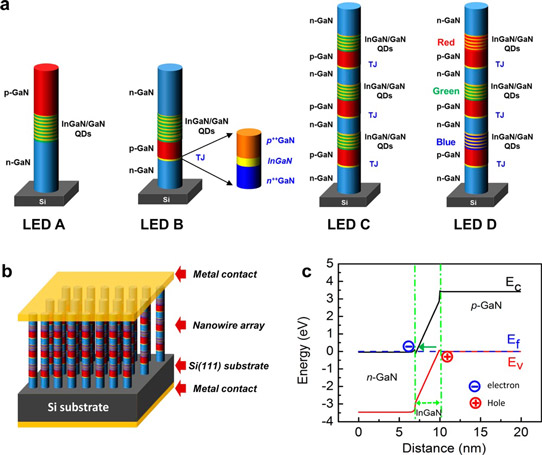
Figure 1: (a) Schematic of dot-in-a-wire LEDs, showing structures of LEDs A, B, C and D. (b) Schematic of fabricated large-area nanowire LEDs. (c) Simulated energy band diagram of GaN/InGaN/GaN tunnel junction showing carrier regeneration and injection process under reverse bias.
The growth conditions were nitrogen-rich. Before III-nitride growth, native oxide on the substrate was desorbed by heating to 770°C. Silicon-doped n-GaN regions were grown at 750°C. The InGaN QDs were created at ~650°C to increase indium incorporation.
The tunnel junctions were also grown at 650°C. These consisted of 12nm of silicon-doped n-GaN, 3nm In0.3Ga0.7N, and 20nm of magnesium-doped p-GaN. The researchers optimized the indium concentrations and layer thickness to achieve maximum tunneling.
"The use of tunnel junction increases the concentration of holes in the p-GaN, thereby minimizing the restriction of low hole injection efficiency in wide-bandgap nitride materials," the researchers explain.
Devices with a single active region (SAR) contained 10 layers of QDs. Multiple active region (3x, MAR) contained 5 layers of QD per active region. The MAR devices could include red, green and blue emitting regions to give phosphor-free white light.
LEDs were fabricated by covering the wires with spin-coated polyimide resist, which was etched back by oxygen plasma to expose the tops of the wires. The p- and n-metal contacts consisted of nickel/gold and titanium/gold, respectively. The respective contacts were made to the top of the nanowires and silicon substrate back-side. The metal contacts for the devices were annealed at 500°C for 1 minute in nitrogen.
The LEDs also included 150nm of indium tin oxide (ITO) as a transparent conducting electrode for current spreading. The indium tin oxide was annealed at 300°C for 1 hour in vacuum.
The turn-on voltages for the single-color LEDs A-C were in order 5.5V, 4.9V and 16V. The relatively high turn-on voltages were attributed to height variations of the nanowires and the formation of silicon nitride insulation at the nanowire-silicon interface.
The researchers comment: "Compared to LED A, LED B shows reduced turn-on voltage, due to the efficient hole injection with the incorporation of tunnel junction and lower contact resistance for n-GaN."
LED B with tunnel junction also showed increased light intensity compared with the reference LED A without tunnel junction. The researchers attribute this to carrier regeneration in the tunnel junction giving multiple opportunities for radiative recombination. The electroluminescence peak was in the green region.
The peak external quantum efficiency occurred at around 50mA for all devices. The researchers comment: "The intriguing part of the result is that, for LED C, the current corresponding to the maximum efficiency point is almost identical to LED A and LED B, suggesting that MAR tunnel junction LED C can be operated at a higher output power while maintaining the same level of efficiency loss of the conventional LEDs."
Thus, efficiency droop occurred at higher input power for the MAR device. At 350mA injection current the output power was a few milliwatts. The researchers suggest that adding a wide-bandgap aluminium gallium nitride (AlGaN) shell to the nanowires could enhance the output power drastically. Such shells are thought to minimize non-radiative surface recombination and increase carrier injection into the active regions.
Temperature-dependent measurements between 80K and 300K (room temperature) on LED C with three active regions showed no significant change in current versus voltage behavior.
LED D with three different wavelength active regions emitted three different colors centered at wavelengths of 445nm, 570nm and 625nm. The color temperature was ~3000K with Commission Internationale de l'éclairage (CIE) chromaticity (x, y) coordinates of (0.47, 0.49) nearly constant over the range 20mA-250mA.
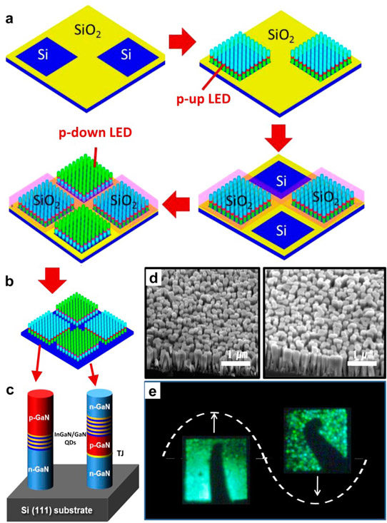
Figure 2: (a) Two-step selective-area growth of p-GaN up and p-GaN down AC nanowire LEDs on Si substrate. (b, c) Device schematics. (d) Scanning electron micrographs (45° tilted) of as-grown p-GaN up and p-GaN down nanowire LED structures. (e) Optical image of green-light-emitting nanowire LED arrays on Si under AC biasing conditions.
The researchers also claim the first AC LEDs with p-GaN up and p-GaN down nanowires on the same silicon substrate (Figure 2). This was achieved through selective-area growth with silicon dioxide masking that was removed with a buffered oxide etch. The device thus emitted green light from different areas with positive and negative polarity.
The performance was tested with AC frequencies between 20Hz and 60Hz and peak-to-peak voltage of 10V.
The researchers believe further optimization of growth and fabrication to make the nanowire height more uniform will lead to more even light emission. Also, higher-frequency operation reduces flicker. The researchers comment: "At a frequency of 60Hz, these devices are almost flicker free and are suited for practical applications."
LEDs on silicon LEDs GaN InGaN PAMBE
http://pubs.acs.org/doi/abs/10.1021/acs.nanolett.5b02515
The author Mike Cooke is a freelance technology journalist who has worked in the semiconductor and advanced technology sectors since 1997.


