


- News
13 November 2015
Magnesium ion implantation of gallium nitride
Hosei University in Japan has claimed the first magnesium (Mg) doping ion implants of gallium nitride (GaN) to show clear rectifying current-voltage behavior, along with ultraviolet (UV) and blue light emission under forward bias [Takuya Oikawa et al, Nuclear Instruments and Methods in Physics Research B, published online 1 August 2015].
Normally, doping of GaN to give p-type hole carriers is achieved during epitaxial growth. This technique is inflexible and results in layers of p-type materials. In mainstream semiconductors, ion implantation is widely used to achieve doping in selected areas of the device through masking that is created in lithography processes. This allows high-performance devices to be created in silicon and silicon carbide.
Previous attempts to transfer ion implant technology to GaN has suffered from the high dislocation density of material grown on sapphire or silicon carbide. While Hall measurements suggested that some of these attempts had produced p-type conversion of the material, devices were not fabricated.
The Hosei researchers used free-standing GaN substrates to grow epilayers of lightly doped n-GaN by metal-organic vapor phase epitaxy (MOVPE). The substrates were separated from their growth substrate by void-assisted separation. The silicon doping concentration in the epilayer was 1x10¹⁵/cm3. The dislocation density was in the 106/cm2 range, rather than the more than 108/cm2 for GaN on sapphire or GaN on silicon carbide.
The samples were prepared for implantation by depositing a 30nm cap layer of silicon nitride. The aim of the cap was to give a maximum Mg concentration at the SiN/GaN interface.
The implantation was carried out in two steps with ion energies of 30keV and 60keV. The respective fluences were 3.5x10¹³/cm3 and 6.5x10¹³/cm3. The implants were annealed at 1230°C for 1 minute in nitrogen.
The researchers fabricated vertical p-n diodes with circular palladium electrodes on the p-GaN contact layer and titanium/aluminium electrodes on the GaN substrate back-side.
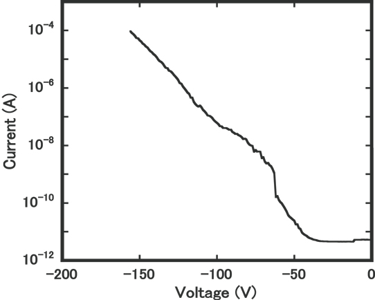
Figure 1: Reverse I–V characteristic of vertical p–n junction diode.
Photoluminescence study suggested that the p-GaN obtained is similar to that produce in MOVPE processes. "These results indicate recovery of lattice damages caused by the Mg implantation and existence of substitutional Mg acceptors in Ga site," the researchers comment.
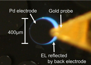 Figure 2: View of light-emitting diode under forward bias. Electrode diameter 400μm.
The pn diode showed rectifying behavior with 4V turn-on. This is higher than the junction value of 3.3V because of series resistance, mainly from an imperfect ohmic contact between the palladium and p-GaN with a Schottky barrier. The reverse leakage current increased from 10-11A to 10-4A between -50V and the -150V breakdown value (Figure 1). The researchers believe the characteristics can be improved by optimizing the Mg-doping profile and the anneal process.
Electroluminescence was also observed with photon energy peaks at 3.1eV and 2.7eV (Figure 2). The 3.1eV UV-A radiation is attributed to acceptor-bound exciton and donor-acceptor-pair emission. "The other peak seems to be Mg-related blue luminescence," the researchers write.
Magnesium doping ion implants of gallium nitride GaN MOVPE
http://dx.doi.org/10.1016/j.nimb.2015.07.095
The author Mike Cooke is a freelance technology journalist who has worked in the semiconductor and advanced technology sectors since 1997.


