


- News
15 May 2015
IBM unveils fully integrated wavelength-multiplexed silicon photonics chip for 100Gb/s transceivers
IBM has designed and tested what it says is the first fully integrated wavelength-multiplexed silicon photonics chip, which will soon enable manufacturing of 100Gb/s optical transceivers.
"Making silicon photonics technology ready for widespread commercial use will help the semiconductor industry keep pace with ever-growing demands in computing power driven by big-data and cloud services," says Arvind Krishna, senior VP & director of IBM Research in Yorktown Heights, NY. "This technology is designed to make future computing systems faster and more energy efficient," he adds.
 Cassette carrying several hundred chips for 100Gb/s transceivers, diced from wafers fabricated with IBM CMOS Integrated Nano-Photonics Technology. (US quarter coin shown for scale.)
Silicon photonics optical components can be used to transfer large volumes of data at very high speed between computer chips in servers, large data-centers and supercomputers, overcoming the limitations of congested data traffic and high-cost traditional interconnects. IBM's new development enables the integration of different optical components side-by-side with electrical circuits on a single silicon chip using sub-100nm semiconductor technology.
The silicon photonics chip uses four wavelengths of light within the optical fiber (rather than traditional copper wiring) to transmit data in and around a computing system. The new transceiver can download an entire high-definition digital movie in just 2 seconds, it is estimated.
The technology industry is entering a new era of computing that requires IT systems and cloud computing services to process and analyze huge volumes of data in real time, both within data-centers and particularly between cloud computing services, notes IBM. This requires that data is moved rapidly between system components without congestion. Silicon photonics greatly reduces data bottlenecks inside systems and between computing components, improving response times, says IBM.
Most of the optical interconnect solutions used within data-centers are currently based on vertical-cavity surface-emitting laser (VCSEL) technology, where the optical signals are transported via multi-mode optical fiber. Demands for increased distance and data rate between ports, due to cloud services for example, are driving the development of cost-effective single-mode optical interconnect technologies, which can overcome the bandwidth-distance limitations inherent to multi-mode VCSEL links.
IBM reckons that, by combining monolithically the essential optical and electrical components of an optical transceiver (as well as structures enabling fiber packaging) onto a single silicon chip, its CMOS Integrated Nano-Photonics Technology can provide a cost-effective solution to extend the reach and data rates of optical links. Also, manufacturing makes use of standard fabrication processes at a silicon chip foundry, making the technology ready for commercialization, reckons IBM.
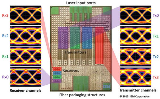
Performance of IBM's fully integrated wavelength multiplexed silicon photonics technology demonstrator chip. Eye diagrams illustrate four separate transmitter channels (right) exchanging high-speed data with four receiver channels (left), each running at 25Gb/s. Credit: IBM.
IBM engineers in New York and Zurich, Switzerland and IBM Systems Group have demonstrated a reference design targeting data-center interconnects with a range up to 2km. The chip demonstrates transmission and reception of high-speed data using four laser frequencies, each operating as an independent 25Gb/s optical channel. Within a full transceiver design, these four channels can be wavelength multiplexed on-chip to provide 100Gb/s aggregate bandwidth over a duplex single-mode fiber, minimizing the cost of the installed fiber plant within the data-center.
IBM presented details of the work at the 2015 Conference on Lasers and Electro Optics (CLEO 2015) in San Jose, CA, USA (10-15 May) in the invited presentation 'Demonstration of Error Free Operation Up To 32Gb/s From a CMOS Integrated Monolithic Nano-Photonic Transmitter'.
IBM attaches silicon photonic chips directly onto processor package
IBM announces $3bn research initiative to tackle chip challenges for cloud and big-data systems
www.research.ibm.com/photonics


