


- News
7 January 2015
Photonic crystal improves light output of InGaN LED by 42% at 350mA
Researchers at Chinese Academy of Sciences’ Institute of Semiconductors have achieved a 42% enhancement in light output from flip-chip indium gallium nitride (InGaN) light-emitting diodes (LEDs) by incorporating a photonic crystal (PHC) structure at the interface between the device and a silver reflector (Figure 1) [Aigong Zhen et al, Appl. Phys. Lett., vol105, p251103, 2014].
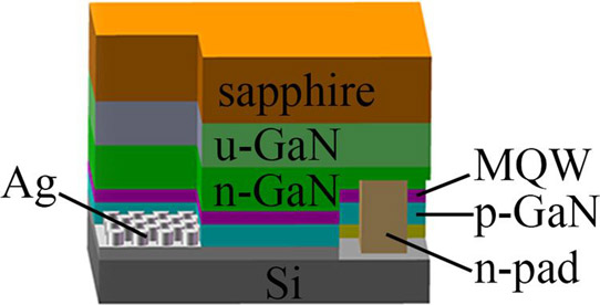
Figure 1: Schematic illustration of FCLED with embedded PHC at the interface of p-GaN and silver (Ag) reflector.
The photonic crystal structure was achieved through lithography using 600nm-diameter polystyrene nanospheres. The spheres were arranged in a single-layer close-packed array, creating a mask for etching hexagonal patterns of holes in the p-type GaN contact layer. The holes were 600nm pitch, 410nm diameter, and 78nm depth. The fill factor of holes was 0.42.
The researchers see their method of producing photonic crystals as more cost effective compared with technologies needing further crystal growth of zinc oxide nanorods or other materials. With InGaN LEDs without light extraction enhancements, some two-thirds of the produced photons can be reflected back into the device, where the energy may be lost through re-adsorption.
The epitaxial material for the LEDs was grown on c-plane sapphire through metal-organic chemical vapor deposition (MOCVD). The epitaxial layers included a 30nm GaN nucleation layer, a 2μm undoped u-GaN buffer layer, a 2μm silicon-doped n-GaN layer, a 180nm InGaN/GaN 450nm-wavelength-emitting multiple quantum well (MQW) layer, a 20nm AlGaN electron-blocking layer, and a 200nm magnesium-doped p-GaN layer.
The epitaxial material was fabricated into 45milx45mil mesa LEDs with a nickel/silver/platinum/gold p-electrode/reflector and chromium/platinum/gold n-electrode. Singulated chips were flipped onto a silicon submount with gold interconnects.
The electroluminescence from the device showed a 42% enhancement in light output power (LOP) at 350mA current injection over a reference ‘planar’ flip-chip LED (FCLED) without photonic crystal. The researchers comment: “The significant improvement in the LOP is mostly attributed to the guide-light diffraction by the embedded PHC structures.”
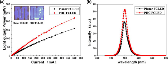
Figure 2: (a) Light output power of PHC FCLED and planar FCLED versus injection current; (b) EL emission spectra of PHC FCLED and planar FCLED at 350mA drive current.
The divergence angle of half intensity of the PHC LED was 145°, compared with 163° for the planar device. The researchers believe that this indicates that the embedded PHC structure serves as a diffraction layer, redirecting light to angles where photons can escape from the top of the chip.
The light extraction efficiency (LEE) enhancement of the fabricated devices was less than suggested by simulations. The researchers comment that this may be due to two factors: “First, the lateral surface of holes is not smooth, which will enhance absorption. Second, the periodicity defects of the PHC structure could weaken the interaction between PHC and guide-light.”
LEDs InGaN InGaN LEDs MOCVD GaN
http://dx.doi.org/10.1063/1.4905030
The author Mike Cooke is a freelance technology journalist who has worked in the semiconductor and advanced technology sectors since 1997.


