


- News
2 December 2015
Mitsubishi uses LayTec in-situ monitoring to grow crack-free GaN-on-Si HEMTs
The main challenge of growing gallium nitride (GaN)-based high-electron-mobility transistors (HEMTs) on silicon substrates is the lattice mismatch between GaN and AlGaN that causes a high tensile stress and often leads to cracks. Now, by using an EpiCurve TT tool from in-situ metrology system maker LayTec AG of Berlin, Germany to monitor surface roughness, growth rate and wafer bowing, Mitsubishi Electric Corp has reported the growth of crack-free low-bowing GaN-on-Si HEMTs by incorporating a GaN buffer layer doped with iron (GaN:Fe), leading to improvements in the breakdown voltage and power-added efficiency (Atsushi Era et al, ICSCRM proceedings (2015)).
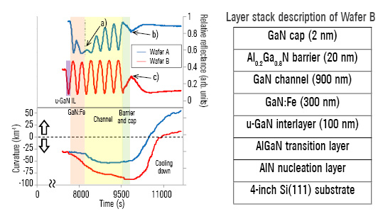
Fig 1: In-situ measurements with EpiCurve TT: (left) reflectance at 950nm and curvature signals during the growth of wafers A and B; (right) layer stack description of wafer B.
Figure 1 (left) shows reflectance and curvature measurements during the growth of wafers A and B. The reflectance of A has a clear slump during the GaN:Fe growth, which indicates a rough surface of the GaN:Fe layer. The compressive stress during the GaN growth of wafer A is obviously insuffiient to compensate the tensile stress during cool-down. The result is cracking over the whole area of wafer A. This is confirmed by the respective atomic force microscopy (AFM) images of surface morphologies (a) and (b) in Figure 2.
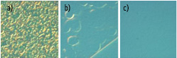 Fig 2: AFM images of surface morphologies: (a) - wafer A directly after GaN:Fe growth, (b) - finished wafer A, (c) - finished wafer B (correlating to a, b, c in Figure 1).
To suppress three-dimensional (3D) island growth in the GaN:Fe, wafer B is grown with a 100nm-thick undoped GaN interlayer (uGaN IL) prior to GaN:Fe growth (Figure 1-right). The reflectance of wafer B shows no slump, which indicates that the GaN:Fe layer grows nicely in two-dimensional (2D) mode. The compressive stress is well balanced, so wafer B is nearly flat after cool-down. Its smooth, crack-free surface is confimed by atomic force microscopy (AFM) – see Figure 2(c). Furthermore, the electron-transfer characteristics of a device fabricated on wafer B exhibit ideal pinch-off behavior.
LayTec Metrology MOCVD GaN HEMTs on silicon
www.laytec.de/power-rf-electronics


