


- News
19 August 2015
Reducing damage in gallium nitride inductively coupled plasma etch
University of California Santa Barbara in the USA and Ecole Polytechnique in France have developed a low-damage dry etch for III-nitride semiconductors that was effective to within 71nm of an active region [Joseph G Nedy et al, Semicond. Sci. Technol., vol30, p085019, 2015]. The process was used on test structures and for creating an air-gap cladding in a laser diode (LD) as an alternative to complex aluminium gallium nitride/gallium nitride (AlGaN/GaN) superlattice (SL) structures.
Dry etching with plasma causes damage with ion bombardment. In many compound semiconductor processes, wet etch is preferred because it causes much less damage. However, for III-nitride semiconductors a simple wet alternative is unavailable.
The test structure consisted of two indium gallium nitride (InGaN) multiple quantum well (MQW) regions grown on double-side polished (DSP) c-plane sapphire (Figure 1). Photoluminescence (PL) from the different depth MQWs was used to analyze the damage from the dry etch procedure.
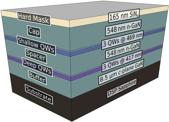
Figure 1. Schematic of c-plane epitaxial growth (by MOCVD) with sputtered SiNx on top and double-sided polished (DSP) sapphire substrate.
The test wafer was cleaved into 6mmx12mm pieces, and mesa stripes were defined by lithographic patterning on the silicon nitride (SiNx) top-layer hard mask. The pattern was transferred to the SiNx with inductively coupled plasma (ICP) etch with trifluoromethane/tetrafluoromethane. The power was low so that the underlying GaN served as an etch stop.
The GaN etching was performed on a Unaxis VLR high-temperature ICP system. The chamber was cleaned and seasoned before the samples were etched. Care was taken to avoid etch byproducts from the silicon carrier wafer and edge effects. A pre-treatment consisting of boron trichloride etch was applied before both the seasoning and main GaN etch runs to remove native oxide and for better etch uniformity.
The GaN etch chemistry was chlorine/argon. Low power was used to minimize sub-surface damage. The ICP was generated at 200W and the forward power was 5W. The low pressure of 2mTorr avoided re-deposition of etch products on the sidewalls and to allow high aspect ratios to be achieved in future. The substrate was heated to 200°C. The etch process parameters were at the lower limit before etch rates became unmeasurable. With the given parameters the etch rate was 26nm/minute on c-plane material.
The use of two MQWs for PL creates an in-situ control, reducing problems from changes in measurement set up and the effects of thinning and surface roughening from the etch. The PL from the deep MQW (417nm) after 500nm etch was a factor of 150% times that of before. The PL from the shallow well (469nm) was therefore normalized according to the change in the PL from the deep well, assuming that it was too far away from the etch to be affected.
The effect of the etch on the shallow-well PL was found to be negligible to within 71nm of this active region. After that point, the PL from the shallow well reduced to near 0% at 25nm, indicating precipitous deterioration of the MQW quality.
Etching into c-plane is expected to be the most difficult, due to 'channeling effects', where ions penetrate more deeply into a crystal lattice in certain directions. The researchers explain: "The crystallographic direction of ion bombardment leads to a greatly elongated tail of ion penetration along the [0001] direction. The c-plane orientation of GaN has the deepest etch damage penetration depth due to channeling effects and is therefore the worst-case scenario for etch damage in a buried active region."
The etch process was applied to an air-gap-cladding (AGC) laser diode structure on m-plane GaN (Figure 2). The upper 275nm of the p-GaN cladding layer was etched with air gaps to create optical confinement in the MQW active region. Etching was also used to create the laser diode ridges. The dielectric isolation material was silicon dioxide. The top p-contact metal was palladium. The facets were also etched, after lithographic patterning.
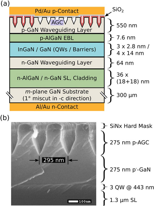
Figure 2. (a) Schematic cross-section of AGC LD design. Lasing direction oriented out of page. (b) SEM micrograph of laser diode ridge cross-section after air-gap dry etch. Air-gap depths outside ridge are 50nm deeper than in ridge.
Applying the etch to the m-plane of the laser diode material, the researchers noticed that the etch rate increased to 45nm/minute and, unlike the c-plane case, there was no preferential etching of pits associated with dislocations.
The aim of AGC was to reduce the overlap of the laser mode with the absorptive p-GaN layer, giving lower threshold gain and higher differential efficiency. The AGC trenches were 150nm wide with 300nm spacing, parallel to the lasing direction. The etching for the AGC was 275nm away from the active region. The researchers report: "Previous attempts at dry-etched features within 300nm reduced the ηIQE and light emission if no subsequent re-growth or anneal was performed. By employing the low-damage dry etch, the active region of this device was unaffected by etch damage."
Room-temperature lasing was achieved at 443nm wavelength with pulsed operation (0.25μsec, 0.25% duty cycle). A 6μmx300μm device had a threshold current density of 26kA/cm2 and differential efficiency from a single facet of 11%. The transition from non-lasing at 90% of threshold was indicated by a narrowing in linewidth from 7.4nm to 2nm above threshold.
In addition to the AGC application, the researchers see potential for the creation of photonic crystals and distributed Bragg reflectors, which could be formed by etching into the top GaN layer to improve LED and laser diode performance.
AlGaN InGaN GaN MOCVD MQW Laser diode
http://dx.doi.org/10.1088/0268-1242/30/8/085019
The author Mike Cooke is a freelance technology journalist who has worked in the semiconductor and advanced technology sectors since 1997.


