


- News
17 November 2014
North Carolina researchers transfer atomic-scale thin films to arbitrary substrates
Researchers at North Carolina State University (NCSU) and the University of North Carolina at Charlotte have developed a new way to transfer thin semiconductor films onto arbitrary substrates, paving the way for flexible computing or photonic devices (‘Surface Energy-Assisted Perfect Transfer of Centimeter-Scale Monolayer and Fewlayer MoS2 Films onto Arbitrary Substrates’ published online on 27 October in ACS Nano; DOI: 10.1021/nn5057673.). The technique is much faster than existing methods and can transfer the atomic-scale thin films from one substrate to others without causing any cracks, it is claimed.
At issue are molybdenum sulfide (MoS2) thin films that are only one atom thick, first developed by Dr. Linyou Cao, an assistant professor of materials science and engineering at NCSU. MoS2 is an inexpensive semiconductor material with electronic and optical properties similar to materials already used in the semiconductor industry.
“The ultimate goal is to use these atomic-layer semiconducting thin films to create devices that are extremely flexible, but to do that we need to transfer the thin films from the substrate we used to make it to a flexible substrate,” says senior author Cao. “You can’t make the thin film on a flexible substrate because flexible substrates can’t withstand the high temperatures you need to make the thin film,” he adds.
Cao’s team makes MoS2 films that are an atom thick and up to 5cm in diameter. The researchers needed to find a way to move that thin film without wrinkling or cracking it (challenging due to the film’s extreme delicacy).
Existing techniques for transferring such thin films from a substrate rely on chemical etching, but the chemicals involved in the process can damage or contaminate the film. Cao’s team has developed a technique that takes advantage of the MoS2’s physical properties to transfer the thin film using only room-temperature water, a tissue and a pair of tweezers.
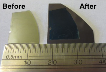 Picture:
Image of thin film on original growth substrate (left) and after being transferred (right). Photo credit: Linyou Cao.
Picture:
Image of thin film on original growth substrate (left) and after being transferred (right). Photo credit: Linyou Cao.
MoS2 is hydrophobic and hence repels water. But the sapphire substrate that the thin film is grown onto is hydrophilic and attracts water. Cao’s new transfer technique works by applying a drop of water to the thin film and then poking the edge with tweezers or a scalpel so that the water can begin to penetrate between the MoS2 and the sapphire. Once it has begun to penetrate, the water pushes into the gap, floating the thin film on top. The researchers use a tissue to soak up the water and then lift the thin film with tweezers and place it onto a flexible substrate. The whole process takes a couple of minutes, whereas chemical etching takes hours.
“The water breaks the adhesion between the substrate and the thin film – but it’s important to remove the water before moving the film,” Cao says. “Otherwise, capillary action would case the film to buckle or fold when you pick it up,” he adds.
“This new transfer technique gets us one step closer to using MoS2 to create flexible computers,” Cao adds. “We are currently in the process of developing devices that use this technology.”
The research was funded by the US Army Research Office under grant number W911NF-13-1-0201 and the National Science Foundation (NSF) under grant number DMR-1352028.
NCSU develops new technique for atomic-layer thin-film growth
http://pubs.acs.org/doi/abs/10.1021/nn5057673
www.mse.ncsu.edu/research/linyou


