


- News
24 December 2014
Double heterostructure with InGaN channel demonstrates high mobility
China’s Xidian University has been developing III-nitride double heterostructures (DHs) with indium gallium nitride (InGaN) channels with a view to high-electron-mobility transistors (HEMTs) [Yi Zhao et al, Appl. Phys. Lett., vol105, p223511, 2014]. The resulting structures boast the highest reported mobility for InGaN channels and superior transport at high temperature, according to the research team.
Nitride semiconductor HEMTs are being developed for microwave power and power switching applications. High-temperature operation could reduce expensive thermal management measures such as cooling or the need for high-thermal-conductivity substrates.
Although single heterostructures (SH) with just a barrier on a buffer/channel layer can achieve higher mobility, high-frequency transistors with short gates fabricated from such materials can suffer short-channel effects that reduce the actual performance far from the ideal. Double heterostructures add a back barrier to block off leakage currents and improve carrier confinement. The DH formation can also reduce short-channel effects such as drain-induced barrier lowering (DIBL) and low punch-through voltages.
The samples (Figure 1) were grown on c-plane sapphire through metal-organic chemical vapor deposition (MOCVD). The transition AlGaN layer was compositionally graded with increasing aluminium content to avoid the formation of a parasitic two-dimensional electron gas (2DEG) in the GaN buffer beneath. The composition grading was also designed to improve the crystal quality of the back-barrier layer.
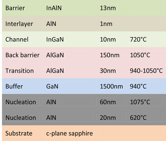
Figure 1: InGaN DH sample structure.
The carrier gas of the precursors into the MOCVD chamber was changed from hydrogen to nitrogen after the back-barrier was deposited. The AlN interlayer between the channel and top barrier was designed to suppress alloy scattering from the InAlN. Reduced electron scattering should improve carrier mobility.
The top InAlN barrier was grown using pulsed MOCVD, alternating the injection of metal-organic precursors and ammonia nitrogen source.
X-ray and photoluminescence analysis suggested that the AlN mole fraction of the AlGaN bottom barrier was 13%. Photoluminescence spectroscopy gave an InN mole fraction of 10% for the InGaN channel.
Room-temperature Hall measurements resulted in an electron mobility value of 1293cm2V-s – claimed as the “highest reported for an InGaN-channel heterostructure”. Sheet resistance from contactless eddy current resistance mapping tests averaged at 289Ω/square with 1.6% wafer uniformity. Capacitance-voltage measurements placed the peak electron density at about 14nm below the sample surface, which corresponds with the 13nm+1nm of the top barrier and interlayer, respectively. The C-V measurements also showed effective suppression of a possible parasitic 2DEG channel in the GaN buffer.
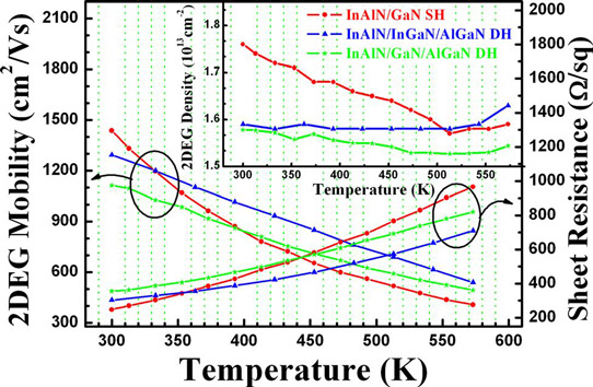
Figure 2: Temperature dependences of Hall mobility and sheet resistance in traditional InAlN/GaN SH sample, InAlN/InGaN/AlGaN DH sample, and InAlN/GaN/AlGaN DH sample. Inset: carrier concentration as a function of temperature.
With a view to power HEMT operation, the researchers also tested the robustness of the channel mobility at elevated temperatures up to 573K (300°C). The sample was compared with InAlN/GaN single- and InAlN/GaN/AlGaN double-heterostructures (Figure 2). At room temperature (300K), the InAlN/GaN single-heterostructure provided the highest mobility of 1437cm2/V-s (247Ω/square sheet resistance). This higher performance is attributed to the absence of a back-barrier and thus of a source of alloy scattering.
All samples showed reduced mobility at high temperature. This was attributed to increased polar optical phonon scattering of electrons. The mobility (and carrier density) of the single-heterostructure sample degraded faster than for the double-heterostructure samples. At 573K, the single-heterostructure mobility was 407cm2/V-s (-70%). The lower mobility and carrier density reduced the conductivity of the single-heterostructure sample, leading to increased sheet resistance at 966Ω/square.
The carrier densities of the double heterostructures were fairly constant over the measured temperature range, indicating good carrier confinement. The InGaN-channel double heterostructure had the higher mobility and carrier density over the range. At 573K, the mobility was 539cm2/V-s, giving a sheet resistance of 711Ω/square. The corresponding values for the GaN double heterostructure were 493cm2/V-s and 820Ω/square.
The researcher suggest that “InGaN channels have the potential to further improve the 2DEG mobility above that of the traditional GaN channels in DHs”.
III-nitride double heterostructures InGaN GaN HEMTs MOCVD
http://dx.doi.org/10.1063/1.4903293
The author Mike Cooke is a freelance technology journalist who has worked in the semiconductor and advanced technology sectors since 1997.


