


- News
1 December 2014
EVG establishes NILPhotonics Competence Center
EV Group (EVG) of St Florian, Austria (a supplier of wafer bonding and lithography equipment for MEMS, nanotechnology and semiconductor applications) has established the NILPhotonics Competence Center, which is designed to assist customers in leveraging EVG’s suite of nanoimprint lithography (NIL) solutions to enable new and enhanced products and applications in the field of photonics. These include light-emitting diodes (LEDs) and photovoltaic (PV) cells, where NIL-enabled photonic structures can improve light extraction and light capturing, respectively, as well as laser diodes, where photonic structures enable the tailoring of device characteristics to improve performance.
The NILPhotonics Competence Center includes dedicated, global process teams, pilot-line production facilities and services at its cleanrooms at EVG’s headquarters in Austria as well as its subsidiaries in North America and Japan.
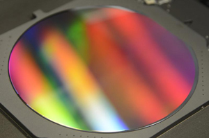 Picture: A 6-inch full-area nanoimprinted wafer processed by EVG NIL solutions.
“Nanoimprint lithography is an enabling technology for the design and manufacture of all kinds of photonic structures, which can significantly shorten time to market and lower cost of production compared to conventional technologies, such as electron-beam writing and stepper systems for optical lithography,” says Markus Wimplinger, corporate technology development and IP director. “For example, compared with conventional lithography, our full-wafer nanoimprinting technology can pattern true three-dimensional structures in the submicron- to nano-range as well as features as small as 20nm, which opens up a range of new photonic applications,” he adds. “With our NILPhotonics Competence Center, we are not just providing our customers with the most advanced NIL systems; we’re also working closely with them during product development to help them determine how best to optimize their product designs and processes to take advantage of the resolution and cost-of-ownership benefits that NIL brings.”
The new center builds on more than 15 years of NIL experience at EVG, which says it has the largest installed base of NIL systems worldwide. The firm’s NIL equipment portfolio includes the recently introduced EVG7200 UV-NIL system, which supports EVG’s next-generation SmartNIL large-area soft NIL process for high-volume manufacturing. The EVG7200 with SmartNIL provides what is claimed to be unmatched throughput and cost-of-ownership advantages over competing NIL approaches.
www.evgroup.com/en/products/lithography/nanoimprint_systems


