


- News
6 August 2014
TU Wien creates ultra-thin solar cells from tungsten diselenide/molybdenum disulphide
Researchers at the Vienna University of Technology (TU Wien) in Austria have combined two semiconductor materials, each consisting of a layer just three atomic thick, to create a new structure that holds promise for a new kind of solar cell, it is reckoned (Furchi et al, ‘Photovoltaic Effect in an Electrically Tunable van der Waals Heterojunction’, Nano Lett., DOI: 10.1021/nl501962c).
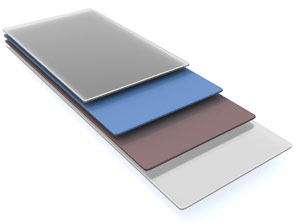 Picture: The solar cell’s layer system: two semiconductor layers in the middle, connected to electrodes on either side.
Several months ago, Thomas Mueller, Marco Furchi and Andreas Pospischil produced an ultra-thin layer of the photoactive crystal tungsten diselenide. Now, this semiconducting material has been combined with another layer made of molybdenum disulphide, creating a structure that could be used in future low-cost solar cells.
Two-dimensional structures
Like other research groups all worldwide, Mueller and his team acquired the necessary expertise to handle, analyse and improve ultra-thin layers by working with graphene. This know-how has now been applied to other ultra-thin materials.
“Quite often, two-dimensional crystals have electronic properties that are completely different from those of thicker layers of the same material,” says Mueller. His team is claimed to be the first to combine two different ultra-thin semiconductor layers and study their optoelectronic properties.
Two layers with different functions
Tungsten diselenide is a semiconductor consisting of three atomic layers: one of tungsten atoms, sandwiched between two of selenium atoms. “We had already been able to show that tungsten diselenide can be used to turn light into electric energy and vice versa,” says Mueller. But a solar cell made only of tungsten diselenide would require countless metal electrodes tightly spaced just a few microns apart. If the material is combined with molybdenium disulphide (which also consists of three atomic layers), this problem is circumvented. The heterostructure can now be used to construct large-area solar cells.
When light shines on a photoactive material, single electrons are removed from their original position, leaving a positively charged hole. Both the electron and hole can move freely in the material, but they only contribute to the electrical current when they are kept apart so that they cannot recombine. To prevent their recombination, metallic electrodes can be used, through which the charge is sucked away - or a second material can be added. “The holes move inside the tungsten diselenide layer; the electrons, on the other hand, migrate into the molybednium disulphide,” says Mueller. Recombination is hence suppressed.
However, this is only possible if the energies of the electrons in both layers are tuned exactly the right way. In the experiment, this can be done by using electrostatic fields. Florian Libisch and professor Joachim Burgdörfer provided computer simulations to calculate how the energy of the electrons changes in both materials and which voltage leads to an optimum yield of electrical power.
Tightly packed layers
“One of the greatest challenges was to stack the two materials, creating an atomically flat structure,” says Mueller. “If there are any molecules between the two layers, so that there is no direct contact, the solar cell will not work,” he adds. Eventually, this was accomplished by heating both layers in vacuum and stacking them in ambient atmosphere. Water between the two layers was removed by heating the layer structure once again.
Part of the incoming light passes right through the material. The rest is absorbed and converted into electric energy. The material could be used for glass frontages, letting most of the light in, but still creating electricity. Also, as it only consists of only a few atomic layers, it is extremely light (300m2 weighs just 1 gram), and very flexible. The team is now working on stacking more than two layers – this will reduce transparency, but increase the electrical power.
http://pubs.acs.org/doi/abs/10.1021/nl501962c


