


- News
3 September 2013
Optimizing spherical cap patterned sapphire for nitride semiconductor LEDs
Researchers in Guangdong province, China, have been exploring the potential for improved light extraction from nitride semiconductor light-emitting diodes (LEDs) on patterned sapphire substrates with spherical cap bumps [Haiyan Wang et al, Jpn. J. Appl. Phys., vol52, p092101, 2013].
Patterned sapphire substrates (PSSs) can improve LED performance by improving the crystal quality of the light-emitting nitride semiconductor material and enhancing light extraction. Gallium nitride (GaN) semiconductor LEDs on flat sapphire suffer from total internal reflection back into the device due to larger differences in refractive index. Patterning can reduce the amount of reflection. Hemispherical and truncated cones are popular shapes for such patterning.
The team from South China University of Technology and NVC Lighting Technology Corporation first performed extensive simulations of different spherical cap geometries to find the optimum radius, height and spacing. The simulations suggested that a 10% enhancement in light output could be achieved with flip-chip packaged LEDs where the radiation is mainly through the substrate and side-walls of the device.
The researchers then prepared two different patterned sapphire substrates: one (HPSS) with 3.45μm-radius hemispherical bumps with 1.6μm edge spacing, and the other an optimized 3.4μm-radius spherical cap (SCPSS) of 2.78μm height with 1.7μm edge spacing (Figure 1). The bumps were arranged in hexagonal arrays to match the crystal structure of the overlying nitride semiconductor material. The patterning was performed by inductively coupled plasma etch where the etch time and plasma flux were controlled.
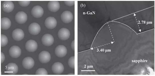
Figure 1: As-prepared spherical cap-shaped PSS. (a) In-plane scanning electron micrograph and (b) low-magnification cross-sectional transmission electron micrograph after epitaxial growth of LED structure.
The researchers point out that, since the etch depth for the SCPSS is less than for HPSS, less photoresist and shorter etch times are required compared with HPSS fabrication. Consequently, fabrication costs would be reduced – a very promising feature for ‘industrial mass production’.
Nitride semiconductor layers were applied using metal-organic chemical vapor deposition (MOCVD). X-ray analysis suggested that the quality of the crystal structures were similar on the different structures, so any difference in performance should be mostly attributed to differences in light extraction and not internal quantum efficiency.
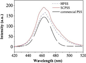 Figure 2: Comparison of EL spectra from LED chips grown on HPSS, up-to-date commercial PSS, and SCPSS.
The electroluminescence (EL) measurements showed a 12% increase in intensity for LEDs produced on the optimized SCPSS substrate (Figure 2). The researchers also compared their devices with LEDs produced on commercial patterned sapphire with cone-shape bumps. The optimized SCPSS LEDs demonstrated a 15% increase in intensity over LEDs produced on commercial patterned sapphire.
LEDs Patterned sapphire substrates GaN MOCVD
http://jjap.jsap.jp/link?JJAP/52/092101/
www.nvc-lighting.com/Index.aspx
The author Mike Cooke is a freelance technology journalist who has worked in the semiconductor and advanced technology sectors since 1997.
