

- News
30 October 2012
SINANO to develop GaN-based power devices with order for two Aixtron MOCVD systems
 Deposition equipment maker Aixtron SE of Herzogenrath, Germany says that in Q3/2012 the Suzhou Institute of Nano-tech and Nano-bionics (SINANO), China, ordered two Aixtron Close Coupled Showerhead (CCS), metal organic chemical vapour deposition (MOCVD) systems for nitride semiconductor research. Deliveries are planned for Q4/2012 and Q1/2013.
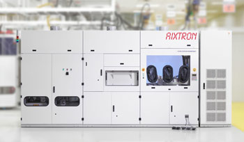
Picture: Aixtron’s CRIUS MOCVD system.
One system, capable of handling 6x2-inch substrates, focuses primarily on R&D, while the other, a CRIUS, is designed for mass production, handling up to 31x2-inch or 3x6-inch substrates in one run.
Dr. Hui Yang, director of SINANO, said: “Our Nano-Devices and Materials Division will use these systems to develop new applications such as gallium nitride (GaN) lasers on the
2-inch R&D system and GaN growth on silicon substrates and high electron mobility transistors (HEMT) on the CRIUS system.”
The Nano-Devices and Materials Division was established in 2006, with one of its research groups focusing on GaN-based high power light-emitting diodes (LEDs) and laser diodes (LDs). The division will now extend its research into the field of power electronics.
GaN-based HEMTs are being widely developed on silicon as a route to mass production of high power density devices for radio frequency and power switching applications.
SINANO Aixtron MOCVD GaN HEMTs