

- News
8 November 2012
Fujitsu’s achieves 2.5kW output from power supply units based on GaN-on-Si devices
Japan’s Fujitsu Semiconductor says it has achieved high output power of 2.5kW in server power-supply units equipped with gallium nitride (GaN) power devices built on a silicon substrate. The firm will exhibit the device for the first time at Embedded Technology 2012 Conference and Exhibition at the Pacifico Yokohama Convention Center in Japan (14-16 November), and will start volume production by second-half 2013.
The use of GaN technology in power supply applications enhances power efficiency and helps to reduce the carbon footprint, notes Fujitsu. Compared with conventional silicon-based power devices, GaN-based power devices feature lower on-resistance and the ability to perform high-frequency operations. These characteristics improve the conversion efficiency of power supply units and make them more compact.
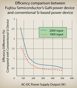 Figure 1: Efficiency comparison between Fujitsu’s GaN power device and conventional Si-based power device.
Fujitsu Semiconductor plans to commercialize GaN power devices on a silicon substrate, increasing the diameters of the wafers and enabling low-cost production. The firm began work on GaN technology in 2009 and has provided specific power-supply-related partners with sample GaN power devices since 2011. Since then, Fujitsu has worked on optimizing them for use in power supply units.
Fujitsu Semiconductor collaborated with Kawasaki-based Fujitsu Laboratories Ltd on several key technical initiatives, including development of the process technology for growing high-quality GaN crystals on a silicon substrate. The collaboration also developed device technologies, such as optimizing the design of electrodes to control the rise of on-resistance during switching, and devising a circuit layout for power supply units that can support high-speed switching of GaN-based devices.
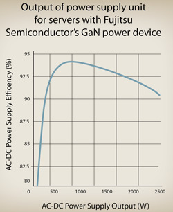 Figure 2: Output of power supply unit for servers with Fujitsu’s GaN power device.
The results have enabled Fujitsu Semiconductor to achieve conversion efficiency that exceeds the performance of conventional silicon devices by using a GaN power device in a power factor correction (PFC) circuit. For example, the firm created a prototype server power-supply unit incorporating a PFC circuit based on GaN technology that achieved output power of 2.5kW. This performance makes GaN power devices suitable for use in high-voltage, large-current applications, the firm reckons.
Fujitsu Semiconductor has established a mass-production line for 6-inch wafers at its Aizu-Wakamatsu plant, and will begin full-scale production of GaN power devices in second-half 2013. It reckons that, by offering GaN power devices optimized for customer applications and technology support for circuit designs, it can support the development of low-loss, compact power supply units for a wide range of uses.