- News
12 March 2012
InAs nickelide meets 12nm ITRS requirements
Researchers based in Belgium, Taiwan, UK and USA have developed a ‘nickelide’ source/drain (S/D) contact scheme for III-V metal-oxide-semiconductor field effect transistors (MOSFET) with a record specific contact resistivity between the contact pad and metallic S/D of 2.7x10⁻⁹Ω-cm2 [R. Oxland et al, IEEE Electron Device Letters, published online 21 February 2012].
Nickelide is a recently developed stable metallic phase formed by reaction of nickel with indium gallium arsenide (InGaAs) III-V compound semiconductor. The new research concerns InAs nickelide and was carried out by TSMC R&D Europe and Hsinchu Taiwan, University of Glasgow, and Texas State University.
In recent years, the use of III-V compound semiconductor channels (Figure 1a) has been widely explored as a means to improve integrated circuit performance. As practical implementation nears, there will be a need to address the practical issue of contacts with the devices. In laboratory devices micron-sized contacts are typical. However, these will need to be reduced to the nanometer scale in practical devices. Reduced size will increase parasitic resistance to impractical levels unless new approaches are developed.
The researchers are developing the technology for the ‘12nm technology generation’ of the International Technology Roadmap for Semiconductors (ITRS). [ITRS has abandoned its traditional ‘technology nodes’ in recent years, given the different pacing of different device types. The time scale for the 12nm processors is given as ~2020 in the 2011 ITRS.] The researchers aimed at meeting the external source/drain resistance figure of 110Ω-μm given in the 2009 ITRS documents.
The team also wants to develop a process that could be implemented in a self-aligned process, analogous to the present self-align silicide (‘salicide’) source/drain contacts used in silicon CMOS production.
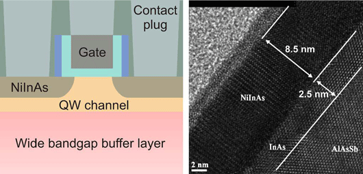
The new contact process was developed on 11nm InAs layers grown on GaAs substrates. The lattice mismatch between the InAs and GaAs materials was bridged “metamorphically” by a 960nm buffer layer of AlAsSb of graded composition. The InAs layer was found to have a surface roughness of 0.61nm in a square field with 10μm sides.
Before electron-beam evaporation deposition of nickel, the InAs surface was cleaned to remove native oxide. The nickel was patterned into various structures using various lithography techniques. The metal was then reacted using rapid thermal annealing (RTA) for 1 minute to create NiInAs. The lowest sheet resistance for a 6nm Ni blanket was achieved with a 350°C RTA process. The resulting NiInAs junction had a depth of around 8.5nm (Figure 1b).
Layer |
Carrier concentration |
Mobility |
Sheet resistance |
11nm InAs channel |
8x10¹¹/cm2 |
4980cm2/V-s |
1428Ω/square |
Reacted NiInAs |
2.2x10¹⁷/cm2 |
0.3cm2/V-s |
110Ω/square |
Table 1: Carrier density, mobility and sheet resistance for InAs channel and nickelide material.
Hall measurements on the pure InAs channel and the nickelide material were performed (Figure 2a). These gave values for carrier density, mobility and sheet resistance (Table 1). The researchers comment: “The observed carrier density and mobility after RTA suggest that the nickelide is metallic. This metallic S/D is a potential solution to the “source starvation” problem for III–V NMOS proposed in [M. V. Fischetti et al, IEDM Tech. Dig., p109, 2007] caused by low density of states in S/D regions.”
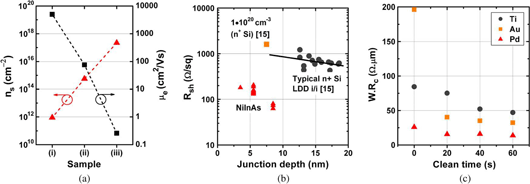
The etch rate of the NiInAs material under hydrochloric acid solution was negligible. Pure nickel with the same solution etches at the rate of 3nm/second. A similar response to such an etch process had been previously found in NiInGaAs. The researchers comment: “It is clear from the atomically abrupt and smooth interface shown in the TEM (Figure 1b), from the comparison with Si Rsh data in Figure 2b and from the availability of a selective wet etch to Ni, that nickelide would make an excellent S/D and extension material for III–V MOSFETs.”
Various metal contact processes were tried. The best contact was achieved using an in situ sputter clean and 10nm palladium metal evaporation. This achieved a transmission line model (TLM) contact resistance of 15Ω-μm before, and down to 5.1Ω-μm after, annealing.
A system with NiInAs and palladium contact metal achieved sheet resistance values of 97Ω/square and 5.1Ω-μm, giving a specific contact resistance of 2.7x10⁻⁹Ω-cm2. The total parasitic resistance due to the metal contact and source/drain extension (Rext) was estimated at 25Ω-μm for an ITRS 12nm device with 23nm contact length and 7nm spacer length.
The researchers believe the contact scheme could be implemented as a self-aligned silicide-like process.
The author Mike Cooke is a freelance technology journalist who has worked in the semiconductor and advanced technology sectors since 1997.