- News
9 March 2012
Nitride HEMT with p-GaN back-barrier and recessing
Researchers in Korea have used p-type gallium nitride (p-GaN) as a back-barrier for recessed-gate high-electron-mobility transistors (HEMTs) [Dong-Seok Kim et al, Jpn. J. Appl. Phys., vol51, p034101, 2012]. The combination of back-barrier and recessing created low buffer leakage and high thresholds up to +2.9V. Nitride HEMTs tend to have negative thresholds, giving normally-on behavior.
The researchers from Kyungpook National University and Electronics and Telecommunications Research Institute aim to develop technology for power-switching applications.
The epitaxial material was grown on (0001) sapphire using metal-organic chemical vapor deposition (MOCVD). The magnesium-doped p-GaN back-barrier was 0.2μm thick. Activation of this layer was performed in-situ by raising the temperature to 800°C. This resulted in a hole concentration of 2x10¹⁷/cm2 and hole mobility of 10cm2/V-s.
The further layers consisted of a 250nm undoped GaN channel, a 1nm AlN interlayer, and a 25nm AlGaN (25% Al) top barrier. This arrangement created a two-dimensional electron gas (2DEG) with mobility and density of 275cm2/V-s and 5.48x10¹²/cm2, respectively. A comparison structure without the p-GaN back-barrier achieved 2DEG mobility and density of 1430cm2/V-s and 1.03x10¹³/cm2.
The thickness of the undoped GaN channel was optimized based on calculations using the depletion model and measurements showing that out-diffusion of Mg from the back barrier occurred to a depth of 100nm. The researchers comment: “If the thickness of the undoped-GaN channel layer is less than 250nm, the current level becomes too low because electrons cannot be sufficiently supplied from the source into the channel owing to the depletion of the 2DEG channel. If the thickness is greater than 250nm, on the other hand, the buffer leakage current will increase, which is undesirable for power-switching applications.”
The epitaxial material was further processed into recessed-gate MOSHFET devices (Figure 1). Mesa and recess etching were performed using a mixed gas plasma of boron tetrachloride and chlorine. Two recess depths were studied: 20nm and 50nm. These resulted in devices with 5nm of the AlGaN barrier left in the first case, and no barrier with further etching into the channel of 25nm in the second case.
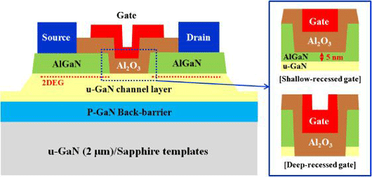
Figure 1: Cross-sectional schematic of fabricated shallow- and deep-recessed GaN MOSHFETs with p-GaN back-barrier.
The 35nm aluminum oxide (Al2O3) gate dielectric layer was deposited using plasma-enhanced atomic layer deposition. Windows were wet etched into the dielectric to allow access to the source/drain regions. The oxide was then annealed at 800°C for 20 minutes in nitrogen.
The source/drain metals consisted of titanium/aluminum/nickel/gold annealed at 750°C for 30 seconds in nitrogen. The gate metal combination was nickel/gold. The gate length and width were 0.25μm and 42μm, respectively.
One expected effect of the back-barrier is reduced buffer leakage. Measurements between two isolated electrodes suggest that the buffer leakage is reduced by three orders of magnitude (a factor of 1000) for the heterostructure with p-GaN back barrier. The back-barrier also reduced current collapse under pulsed operation to 8.9%, compared with 48% for the device without back-barrier.
The different gate recess depths affected the threshold voltage. The shallow recess resulted in a threshold of +0.8V, while the deeper recess gave a value as high as +2.9V. Such high thresholds are needed to avoid switching error and ensure safe normally-off operation.
The disadvantage of deep recessing is a lower maximum drain current and transconductance of 90mA/mm and 30mS/mm, respectively, at drain bias of 6V, compared with 255mA/mm and 52mS/mm for the shallow recessed device.
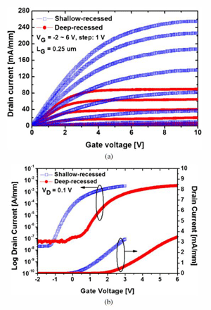 The researchers blame decreased channel electron mobility and degraded gate oxide interface quality due to the prolonged recess etch. The field-effect mobility was estimated at 25cm2/V-s for shallow recessing and 9cm2/V-s for deep recessing. The interface trap densities were 4.72x10¹²/eV-cm2 and 7.03x10¹²/eV-cm2, respectively. This reduced interface quality also impacted on/off current ratios (Figure 2).
Figure 2: (a) DC characteristic and (b) linear and logarithmic transfer I–V characteristics in the linear region at drain bias of 0.1V for shallow- and deep-recessed devices.
Despite the degraded performance, the researchers see increased threshold as “one of the most important issues in GaN power-switching applications”. They add: “The device performance can be improved by applying a post-surface treatment to recover the damage and smooth the surface.”
The off-state breakdown for 1mA/mm leakage at 0V gate potential was around 70V with a gate-drain spacing of 3μm. The researchers comment: “We believe that this low breakdown voltage may be attributed to the oxide breakdown caused by the strong electric field at the drain edge of the gate electrode for such a small gate-to-drain spacing, rather than normal drain breakdown due to impact ionization. The breakdown voltage can be increased by simply increasing the gate-to-drain distance or by adopting appropriate device designs, such as a field plate or a double recess process.”
Flattening transconductance profiles in nitride HEMTs
Aluminum oxide passivation reduces off-current in AlN/GaN transistors
Nitride HEMT p-GaN back-barrier AlGaN MOSHFET MOCVD Sapphire substrates
The author Mike Cooke is a freelance technology journalist who has worked in the semiconductor and advanced technology sectors since 1997.