- News
27 March 2012
All-ternary InAlAs/InGaAs DHBT high frequency and breakdown performance
The UK’s University of Manchester has produced all-ternary indium aluminum arsenide/indium gallium arsenide (InAlAs/InGaAs) double-heterojunction bipolar transistors (DHBTs) that achieve simultaneous high breakdown voltages (5.5V) and cut-off frequencies (140GHz) [R Knight et al, Semicond. Sci. Technol., vol27, p045017, 2012].
Single-heterojunction devices can achieve higher cut-offs of 550GHz, but have poorer breakdown behavior. Good breakdown characteristics are needed for high-power or precision mixed-signal performance. Higher breakdowns of 4.0-4.5V and high cut-offs of 560GHz have been achieved in the USA with indium phosphide/indium gallium arsenide (InP/InGaAs) DHBTs produced using sub-micron electron-beam or deep ultraviolet lithography.
The University of Manchester (UoM) device uses micron-scale optical lithography. The team has worked in the past few years on the InAlAs/InGaAs combination to overcome current-blocking affects that arise from a large discontinuity between the base-collector conduction bands, compared with InP/InGaAs-based devices. The team has developed designs with composite collector and doping interface dipole structures to achieve this aim. In particular, they have avoided the use of more complex (and hence more costly to manufacture) quaternary InAlGaAs material structures.
The Manchester work was supported by European defense electronics company Selex Galileo and the UK Electro-Magnetic Remote Sensing Defence Technology Centre (EMRS DTC). Partial funding also came from the UK Science and Technology Facilities Council (STFC) as part of the Square Kilometre Array (SKA) radio telescope program.
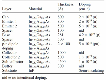 The epitaxial structure (Table 1) was grown on 3-inch iron-doped indium phosphide substrates using solid-source molecular beam epitaxy (SS-MBE) in a Riber V90H system. The growth temperature was a low 420°C in order to limit the diffusion of the beryllium doping from the p-type base layer. The n-type doping was achieved using silicon. The layers were lattice matched to the substrate so that InAlAs layers had 52% In molar fraction, and InGaAs layers 53%, except for base grading from 53% at the collector junction to 46% at the emitter junction.
Table 1: Epitaxial structure of DHBT.
Triple-step mesas were etched, allowing access to the emitter, base and collector regions with ohmic palladium/titanium/palladium/gold contacts. Further interconnects were non-alloyed titanium/gold deposited on benzocyclobutene (BCB) passivation. The base metal layer incorporated an air-bridge structure to minimize base-collector capacitance.
A 1μm x 5μm device gave a current gain of 42, an offset voltage of 350mV, power handling of 10mW, and current density of 1mA/μm. The breakdown voltage for 100μA collector current was 5.5V.
The peak RF performance was achieved at 4.2mA collector current and a collector-emitter voltage of 2V. The unity-gain cut-off (fT) and maximum oscillation (fmax) frequencies came at 140GHz and 95GHz, respectively.
The researchers compared their device with those available commercially (Table 2). Although the Manchester device does not exceed the current performance of the commercial products, the researchers are hopeful that with “further epitaxial design work and investment to reduce device geometries, this material system may prove to have RF performance useful for high-frequency power applications”. The new DHBT is also “the start of a UoM InAlAs-InGaAs BiFET and MMIC fabrication process.”
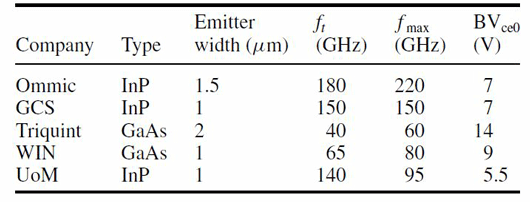
Table 2: Commercially available InP and GaAs DHBTs. Last line is University of Manchester’s device.
The researchers conclude: “The demonstration of the frequency performance whilst achieving large breakdown voltage of 5.5 V coupled with the ease of processing makes the reported all-ternary InGaAs–InAlAs DHBTs attractive candidates for a number of high-power MMICs and BiFET applications.”
www.selexgalileo.com/SelexGalileo/EN/index.sdo
The author Mike Cooke is a freelance technology journalist who has worked in the semiconductor and advanced technology sectors since 1997.