- News
16 March 2012
Aixtron Training and Demonstration Center opens at SINANO in Suzhou
 To mark the opening of its new training and demonstration center at SINANO - the Suzhou Institute for Nanotechnology and Nanobionics, deposition equipment maker Aixtron SE of Herzogenrath, Germany has held a ceremony in the city of Suzhou, China, attended by a representative of the National Development and Reform Commission (NDRC), the German Consul General in China, many of Aixtron’s key customers, and numerous partners from leading universities and research institutes from across Greater China.
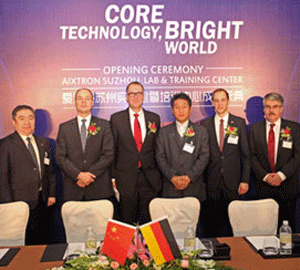
Picture: Left to right: Lionel Chen and Dr Bastian Marheineke (both Aixtron), Wolfgang Breme (CFO Aixtron), professor Hui Yang (director SINANO), and Dr Nicolas Muesgens and professor Michael Heuken (both Aixtron).
At the Suzhou Industrial Park (SIP) in the Yangtze River Delta – which Aixtron describes as one of China's most influential business locations – future Chinese MOCVD experts will be trained in the latest semiconductor technology and manufacturing processes. The Aixtron center will be able to draw upon the collaborative synergies between industrial and institutional research and will also offer a high quality of training, says Aixtron.
“In order to achieve China’s aim of global LED leadership, LED products made in China need to be able to take the lead in lighting quality, efficiency and cost-effectiveness. This cooperative arrangement will make a significant contribution toward achieving these goals,” says a spokesperson for SINANO. “One of the new facility’s main priorities will be to provide Chinese customers with the depth of process knowledge they need in order to optimize their devices,” they add.
“China is now playing a significant global role in the emergence of the LED lighting market through the extensive national and regional encouragement of LED applications,” said Aixtron’s president & CEO Paul Hyland at the ceremony. “At the new center, we will be able to proactively support our customers’ technology developments by utilizing the very latest Aixtron technologies and by providing the highest-quality training, not only in the field of LEDs but also in other nanotechnology areas, including GaN-on-Si,” he adds. The cooperative agreement with SINANO will facilitate the full process and characterization of LEDs, the technical properties of which are essential to lighting product quality, says the firm.
The training courses offered will use Aixtron’s latest-generation CRIUS II-XL and AIX G5 HT MOCVD systems and will be held in a production cleanroom environment, laboratories, and classroom training facilities that occupy a total area of 350m2. “We will focus on the most critical factors in the manufacturing process, which will enable operators of MOCVD facilities to achieve better system utilization times and higher yields, thereby reducing their operating costs – our focus will be on operational efficiency, maintenance routines, process optimization and fab management,” says Dr Nicolas Muesgens, director of the Aixtron Training and Demonstration Center. “In Suzhou, we will offer intensive, science-based, hands-on training courses to small groups, led by Aixtron’s highly qualified and experienced engineers,” he adds.
Aixtron says that, as well as its focus on best-practice commercial considerations, the new training center will also pay special attention to operational health and safety issues and to the protection of the environment, by adhering to and promoting German, international and Chinese product-safety and waste-management standards.
Applications to attend a training course can be submitted online at: www.aixtron.com/Service/Training.