- News
20 June 2012
NXP highlights GaN portfolio at IMS, targeting ‘mainstream GaN’
Recognized as a compelling alternative to silicon for many RF applications, gallium nitride (GaN) technology has generated significant industry interest due to its performance advantages, but has faced significant challenges related to cost, says NXP Semiconductors N.V. of Eindhoven, The Netherlands, which provides mixed-signal and standard product solutions. In booth 607 at the 2012 IEEE MTT-S International Microwave Symposium (IMS) in Montreal, Canada, NXP is demonstrating its full portfolio of first-generation GaN products, and discussing its vision and roadmap related to GaN. Core to that vision, says the firm, is the concept of ‘mainstream GaN’ - bringing economies of scale and over 30 years of experience in RF power transistors to facilitate a secure, reliable supply chain for RF GaN products.
 “Since announcing our commitment to ‘mainstream GaN’ last year, we’ve received a great deal of interest in our GaN offerings and have worked intensively with a handful of key customers to refine our first-generation GaN portfolio,” says Mark Murphy, director of marketing, RF power product line. “At the same time, by offering our customers a choice between high-performance GaN and LDMOS - and in some situations a mix of both – we’re in the unique position of being able to offer unbiased choices for fully optimized designs, depending on the specific requirements of each application,” he adds.
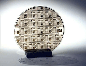
Picture: A GaN wafer fabricated by NXP.
NXP currently offers engineering samples of its first-generation GaN products, including the CLF1G0035-50 and CLF1G0035-100 amplifiers for 50W and 100W broadband applications. At IMS2012, NXP is demonstrating live application examples, including a multi-stage GaN line-up covering a 200-2700MHz frequency band. Using the new CLF1G0060-10 driver, as well as the CLF1G0035-50 amplifier for the output stage, the GaN line-up features 50V GaN technology and what is claimed to be best-in-class linearity. Due to the higher impedance levels of the 50V GaN process, broadband amplifiers can be designed on a single transistor.
Based on a 0.5µm gate-length technology developed in collaboration with the Fraunhofer Institute for Applied Solid State Physics (Fraunhofer-IAF) in Freiburg, as well as United Monolithic Semiconductors (UMS) in Ulm, Germany, NXP’s first-generation GaN amplifiers feature what is claimed to be excellent linearity without compromising power, ruggedness and efficiency, significantly reducing component count and amplifier footprint. The collaboration with UMS and Fraunhofer IAF Institute also establishes a Europe-based supply chain for GaN technology.
NXP will be ramping up for volume production and offering engineering samples of additional GaN amplifiers in Q3 and Q4/2012.
At IMS 2012, NXP is also highlighting applications using GaN, including a live Class E amplifier tuned for 2.45GHz, showing the efficiency enabled by GaN. Featuring a transistor with internal Class E harmonic matching, the amplifier achieves efficiency of 75.2% at 24W. Based on a 0.25µm gate-length technology currently under development, NXP plans to make its high-efficiency Class E narrow-band GaN solutions available in 2013.
NXP is also developing a digital power amplifier using GaN switching transistors that offer higher efficiency than linear amplifiers. These switched-mode power amplifiers (SMPAs) can be used in multiple bands without any modification to the hardware, and will be a key driver of the ‘ultimate’ base station of the future, reckons the firm. Like its other GaN processes, the 0.25µm GHSM process uses SiC substrates for better reliability, superior RF performance, and enhanced thermal management, underscoring the advantages of an unbiased approach to GaN, the firm adds.
NXP says that, while RF GaN has already gained significant traction in the aerospace and defense market, it is also focusing on future growth areas including wireless infrastructure and base stations, energy transfer, and the sensing and imaging markets.
