- News
13 June 2012
IQE enhances test & measurement capabilities with Nanotronics automated wafer inspection tool
 Epiwafer foundry and substrate maker IQE plc of Cardiff, Wales, UK says that it has enhanced wafer inspection capabilities at its Cardiff facility by acquiring a new automated wafer inspection tool supplied by Nanotronics Imaging LLC of Cuyahoga Falls, OH, USA.
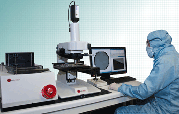
The nSPEC tool enhances existing manual microscopy inspection by allowing automated loading and scanning of III-V semiconductor wafer products including gallium nitride (GaN), gallium arsenide (GaAs) and indium phosphide (InP)-based materials. The tool has built-in intelligence to enable repeatable and quantifiable object recognition to identify, categorize and record wafer features in real-time.
The acquisition of the tool follows an extensive six-month evaluation where the reliability and repeatability was compared with existing inspection techniques. This is the second nSPEC tool to be installed at IQE, the first unit having been commissioned and in use at the its manufacturing facility in Somerset, NJ, USA.
“The new automated inspection system offers a compelling alternative to manual microscope inspection, with greater repeatability and significantly reduced chance of human error,” comments Eliot Parkinson, general manager of IQE’s III-V manufacturing facility in Cardiff.
“Rapid inspection that gives repeatable and useful results needs to be thought of as a modern technology like the personal computer used to be, and the smart phone is now. What has traditionally been too expensive, too complicated, and provided too little relevant information now needs to have all required features and more, so that all companies using wafer inspection tools can have best-in-class technology that is affordable,” says Nanotronics Imaging’s CEO Matthew Putman. “We are at a point of technological convergence, where our engineers can develop such a tool. We are also pleased to have worked with a global leader like IQE to evaluate our tool in a high-volume semiconductor wafer manufacturing environment,” he adds.
Nanotronics launches nSPEC automated wafer inspection system
IQE Nanotronics Wafer inspection