- News
26 January 2012
SiO2/GaN nano-rods give new base for high light output power
National Chiao Tung University researchers in Taiwan have improved nitride semiconductor light-emitting diode (LED) performance by growing the structures on silicon dioxide on gallium nitride (SiO2/GaN) nano-rods [Ching-Hsueh Chiu et al, Nanotechnology, vol23, p045303, 2012]. The effect is to produce nano-scale epitaxial lateral overgrowth (NELOG) material with lower densities of dislocations, boosting light generation, and to create a reflective bottom layer of air-voids that improves light extraction through the top of the device.
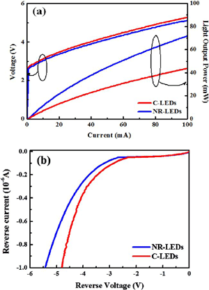
At 20mA, devices grown on nano-rods reduce the forward voltage to 3.37V and have light output power of 21.6mW, compared with a conventional device that offers 3.47V and 13.1mW, respectively. The researchers believe that improved material quality (i.e. reduced dislocations) and light extraction explain these results. A reduction in dislocation densities is also suggested by a reduced reverse bias leakage current. Simulations suggest a 1.45x enhancement in light extraction from reflection by the nano-rod layer. Measurements gave a smaller boost of around 30% (1.3x), which the researchers suggest may be due to imperfections of the air-void shapes and sizes, compared with a simulation.
 The nano-rods/air-voids are formed by first plasma-enhanced chemical vapor depositing 200nm SiO2 on a 2μm GaN-on-sapphire layer, followed by evaporation of a 10nm nickel mask. The structure was then annealed at 850°C for one minute. The 250–500nm diameter nano-rods (NRs) were formed by reactive ion etch of the SiO2 (carbon tertrafluoride, 3min) and inductively coupled plasma etch of the GaN (chlorine/argon, 34min). A heated nitric acid dip was used to remove nickel residue.
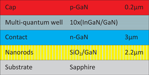
Figure 1: Epitaxial structure grown on SiO2/GaN nano-rods.
The process resulted in a nano-rod density of 3.3x10⁸/cm2. Further nitride semiconductor layers (Figure 1 and 2) were then grown on the nano-rods using a Veeco metal-organic chemical vapor deposition (MOCVD) system. Comparison devices without nano-rods were also produced.
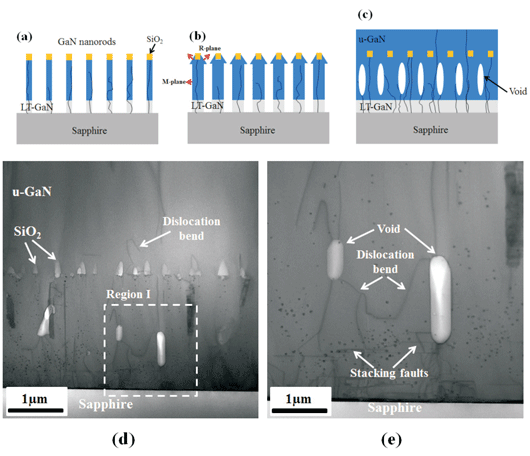
Figure 2: Procedure for air-void formation between a GaN NRs and u-GaN epitaxial layer. (d) TEM image of GaN epilayer overgrowth on GaN NRs, (e) HRTEM image of region I in (d). The diffraction condition is g = 0002.
 One effect of growing epitaxial layers on the nano-rods was to reduce threading dislocation densities (TDDs) to around 5x10⁷/cm2. Electron microscopy suggested that the TDD reduction can be attributed to misfit and dislocation bending just above the air-voids. Also, Raman scattering analysis that reveals phonon/sound-wave characteristics and hence stress in the material showed a reduction in residual stress in the epitaxial GaN from 1.73GPa in material without air-voids to 0.88GPa with air-voids.
Photoluminescence measurements were used to derive internal quantum efficiencies (IQEs) of 46% for the conventional LED and 53% for the air-void device (a15% enhancement). Combining this with the simulated improvement in light extraction of 1.45x gives a 67% increase in performance, compared with the measured result of 65% (1.65 = 21.6/13.1).
Figure 3: (a) Forward voltage and light output power characteristics with drive current of fabricated LEDs. (b) Reverse voltage characteristics.
http://iopscience.iop.org/0957-4484/23/4/045303/
The author Mike Cooke is a freelance technology journalist who has worked in the semiconductor and advanced technology sectors since 1997.