- News
10 April 2012
Polarization matching as a route to nitride semiconductor transistor enhancement
Germany’s RWTH Aachen University and Fraunhofer IAF (Institute for Applied Solid State Physics) have applied nitride-semiconductor polarization engineering to create enhancement-mode (normally-off) field-effect transistors [Herwig Hahn et al, Semicond. Sci. Technol., vol27, p055004, 2012].
There has been much recent research in shifting the thresholds of nitride transistors from negative to positive values, giving enhancement-mode rather than depletion-mode (normally-on at zero gate potential). Advantages of normally-off devices include lower power consumption and fail-safe behavior. The fail-safe characteristic is especially desirable for the high-power/voltage applications that are among the attractions of wide-bandgap nitride semiconductor devices.
RWTH and deposition equipment manufacturer Aixtron have recently developed quaternary aluminum indium gallium nitride (AlInGaN) barrier layers that can be polarization-matched to GaN buffers. This can allow normally-off conduction while maintaining a suitable conduction band offset, if the polarization-matched barrier is compressively strained. The compressive strain requires rather high indium contents. Previous work with AlInGaN in transistor structures contained only around 2% In.
The RWTH/Fraunhofer devices are the first compressively strained, nearly polarization-matched AlInGaN/GaN metal insulator semiconductor heterostructure field-effect transistors (MISHFETs) to be presented. The In-content of these devices was around 20%.
The epitaxial material was grown on c-plane sapphire using an Aixtron metal-organic chemical vapor deposition (MOCVD) reactor. A thin AlN spacer layer separated the 2μm GaN buffer from the compressively strained AlInGaN barrier. The barrier was grown at 716°C using continuous (sample A) and pulsed (sample B) methods. The pulsing of the Ga precursor resulted in enhanced In incorporation. The barrier compositions were Al0.48In0.18Ga0.34N and Al0.57In0.23Ga0.20N for samples A and B, respectively.
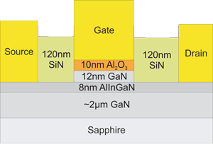 To construct HEMTs (Figure 1), the epitaxial material was covered in aluminum oxide (Al2O3) before gate metallization. The Al2O3 was deposited using atomic layer (ALD) techniques. The gate metal was nickel. The gate was then used as a hard mask to etch down to the AlInGaN layer away from the gate region. Ohmic titanium/aluminum/titanium/gold was used to provide source-drain contacts. Silicon nitride was then applied as passivation.
Figure 1: Structure of the gate-first processed samples.
The device geometry consisted of 2x50μm-wide, 1μm-long gates. The gate-source distance was 1.5μm and the gate-drain distance was 2.5μm.
The drain currents at 4V gate potential and 10V drain bias were 115mA/mm and 27mA/mm for HEMTs based on samples A and B, respectively. The low current in HEMT B is attributed to high sheet resistance in the source-drain access regions (Table 1). The maximum transconductance values were 40mS/mm for sample A HEMTs and 10mS/mm for sample B.
Data |
Sample A |
Sample B |
Contact resistance |
~5Ω-mm |
~5Ω-mm |
Sheet carrier concentration |
6x10¹²/cm2 |
1.2x10¹²/cm2 |
Sheet carrier mobility |
450cm2/V-s |
215cm2/V-s |
Sheet resistance |
2.2kΩ/sq |
22kΩ/sq |
Barrier/buffer polarization charge difference |
0.0041C/m2 |
0.0014C/m2 |
Table 1: Data from calculations, van-der-Pauw, Hall and transmission-line model (TLM) measurements.
The threshold voltages were positive in both cases, giving enhancement-mode, normally-off behavior. The HEMT A threshold was 0.56V, lower than that for sample B-based devices at 0.96V. The higher threshold from sample B was attributed to a reduction in polarization charge density from the polarization field between the buffer and barrier layers. A lower charge reduces the carrier density in the two-dimensional electron gas (2DEG) channel. This also increases the source-drain access sheet resistance.
The researchers comment: “Better results can be expected with optimizations concerning not only the mobility in the 2DEG, but also the improvement of the contact resistance”.
The presence of the Al2O3 gate insulation reduces gate leakage currents (compared with normal Schottky-gate devices) at 4V gate potential to less than 1μA/mm for HEMT A and less than 100nA/mm for HEMT B.
The three-terminal off-state (0V gate) breakdown was 105V for HEMT A. This increased to 405V for a device with a gate-drain distance of 20μm. The high values are attributed to the gate insulator and high buffer quality. Sample B devices had breakdowns up to 490V. “The values shown here are valid for devices without a field-plate. The addition of a field-plate and thus the reduction of the peak electric field would enhance the breakdown voltage even further,” the researchers say.
The stability of the threshold voltage was also studied for the better performance devices based on sample A. Sweeps in gate voltage in the negative (+4V to -8V) and positive (-8V to +4V) showed a small amount of difference in the subthreshold region that was more visible in the transconductance as opposed to the drain current.
Further tests involved applying stresses (+4V or -8V) to the gate for extended periods of time (up to 1000 seconds). The +4V, 1000s stress shifted the threshold up to +1.53V, while the -8V, 1000s stress shifted the threshold down to +0.35V. Despite the shift down, the threshold was still in the positive enhancement range.
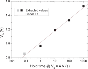 The researchers suggest that the positive gate bias drives electrons into acceptor-like traps at the Al2O3 interface, depleting the 2DEG channel under the gate. The negative bias, by contrast, de-traps electrons in these states. A logarithmic dependence of the threshold shift on hold time (Figure 2) was seen by the researchers as being consistent with a tunneling process.
Figure 2: Dependence of threshold voltage on hold time, when devices are held at 4V gate potential. The 75ms time is estimated and indicated as a grey dot.
Before the devices become competitive, the researchers say that they will need to optimize the ohmic contacts and improve the 2DEG mobility. “Nonetheless, as quaternary nitride structures can be grown on large-diameter silicon substrates, this technology could pave a way for enhancement-mode high-power high-voltage GaN-based power switches,” they conclude.
E-mode FETs HEMT AlInGaN barrier layers GaN Sapphire substrates Aixtron
The author Mike Cooke is a freelance technology journalist who has worked in the semiconductor and advanced technology sectors since 1997.