- News
21 October 2011
Back-barrier boosts nitride HEMT cut-off frequency
Massachusetts Institute of Technology, IQE RF LLC and University of Notre Dame have used an indium gallium nitride (InGaN) back-barrier to control short-channel effects (SCEs) in indium aluminum nitride/gallium nitride (InAlN/GaN) high-electron-mobility transistors (HEMTs) “for the first time” [Dong Seup Lee et al, IEEE Electron Device Letters, published online 19 September 2011].
The researchers used the back-barrier structure to achieve a record current-gain cut-off frequency (fT) of 300GHz for lattice-matched InAlN/GaN HEMTs with 30nm gate length. The group expects that “improved suppression of SCEs at this gate length in combination with reduced access resistance will enable even better performance in the future”. The team compares its result with the achievement of 225GHz fT for AlGaN/GaN HEMTs.
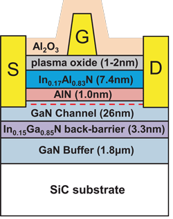 The MIT/IQE/Notre Dame devices (Figure 1) were grown on silicon carbide (SiC) substrates, using metal-organic chemical vapor deposition (MOCVD). The InGaN back-barrier has a polarization-induced electric field that creates an effective conduction-band offset. Hall measurements give a two-dimensional electron gas (2DEG) carrier density of 1.65x10¹³/cm2 and electron mobility of 1581cm2/V-s. By contrast, an AlGaN back-barrier creates a polarization-induced electric field in the GaN channel layer.
Figure 1: Schematic of MIT/IQE/Notre Dame InAlN/GaN HEMT with lattice-matched InGaN back-barrier.
The device processing consisted of mesa isolation through boron trichloride-chlorine plasma etch, silicon-germanium-titanium-aluminum-nickel-gold ohmic contact deposition and 820°C annealing, oxygen plasma treatment of the top InAlN epitaxial layer to reduce gate leakage and improve RF performance, deposition of a rectangular nickel-gold gate and, finally, aluminum oxide passivation.
One disadvantage of a rectangular gate, as opposed to the more usual mushroom/T-gate, is higher gate resistance that results in poor power-gain. On the other hand, parasitic gate capacitance of the device is reduced, allowing the researchers to push the current-gain to its limit. The poor power-gain is presumably one reason why the power-gain cut-off (fmax) is not reported. In AlGaN/GaN and AlN/GaN fmax values have been reported up to 400GHz.
The source–drain distance of the MIT/IQE/Notre Dame devices was 1μm. The gate length was varied between 30nm and 230nm.
In terms of DC performance, the devices showed more evident short-channel effects (SCEs) below 50nm gate length: for example, the threshold voltage rolled-off in a more negative direction for devices below this point. The drain current of a 30nm-gate device at 0V gate potential can reach 1.8A/mm; the on-resistance was 1.2Ω-mm. The peak extrinsic transconductance was 529mS/mm with drain bias 3V. The researchers extracted a threshold voltage of –4.21V at the same bias.
Above 70nm, the researchers see effective suppression of SCEs due to the combination of a back-barrier and a thin GaN channel, despite the relatively thick top AlN/InAlN/plasma oxide barrier of about 10nm.
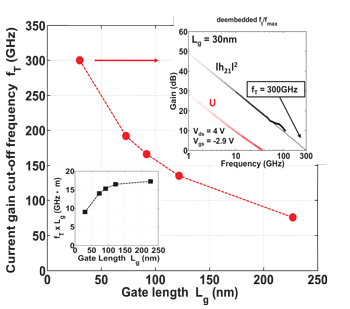 The RF performance was tested between 110MHz and 110GHz (Figure 2). Parasitic pad capacitances and inductances were de-embedded using off-wafer line reflect match calibration standards and on-wafer open and short structures. The fT of the 30nm device of 300GHz is described as “the highest value reported in GaN-based transistors so far”, according to the researchers’ knowledge. Figure 2 suggests an fmax value of tens of GHz.
Figure 2: Current-gain cutoff frequency (fT) vs gate length (Lg). Top inset, RF performance of 30nm gate-length device with 300GHz fT. Bottom inset, fTxLg dependence on Lg.
Despite this record result, the product of this value with the gate-length (Lg) was 9GHz-μm, about half the value for a 230nm device (17.3GH-μm). In the absence of SCEs, one would expect the value of fTxLg to remain relatively constant as the gate length is reduced. The researchers comment: “This decrease is mainly due to the total delay becoming dominated by extrinsic and parasitic components.”
Electron velocity determinations were made based on parasitic charging delay and intrinsic gate capacitance variation with Lg, both extracted at the effective bias condition, giving values of 1.37x107cm/s and 1.45x107cm/s, respectively.
Funding for the research came from the US military research funds for the DARPA NEXT and ONR DURIP programs.
MIT IQE InAlN/GaN HEMTs InGaN SiC substrates MOCVD
The author Mike Cooke is a freelance technology journalist who has worked in the semiconductor and advanced technology sectors since 1997.