- News
20 May 2011
Piranha gobbles up hysteresis of aluminum oxide nitride semiconductor interface
US Naval Research Laboratory researchers (with Nelson Y. Garces of Global Strategies Group) have been studying ways to improve the quality of aluminum oxide (Al2O3) grown on gallium nitride (GaN) by atomic layer deposition (ALD) [Neeraj Nepal et al, Appl. Phys. Express, vol4, p055802, 2011]
Aluminum oxide is of interest as a gate insulator for high-frequency, or high-power, nitride semiconductor transistors to reduce gate leakage currents compared with devices that use a direct Schottky metal gate contact with the semiconductor barrier. Other advantages of an insulated gate are higher breakdown voltages and higher channel current.
However, producing a high-quality insulator–semiconductor interface is tricky. In particular, one needs to avoid charge traps and fixed charges from developing that adversely affect device performance. For this, some surface preparation of the semiconductor surface before deposition is needed. For convenience, it is preferable to perform this preparation in the deposition chamber itself, rather than having to use an external process.
A popular technique for creating Al2O3 films is atomic layer deposition. Surface preparation in such chambers requires a relatively low-temperature process.
Three pre-treatments were studied: hydrogen peroxide–sulfuric acid (H2O2:H2SO4, 1:5), hydrofluoric acid solution (H2O:HF, 1:1), and hydrochloric acid solution (H2O:HCl, 1:1). Hydrochloric acid is commonly used as a native oxide etchant for GaN (e.g. for removal of oxides that form on exposure to air). The acid solution treatments were carried out for one minute at room temperature. The hydrogen peroxide–sulfuric ‘piranha’ treatment lasted for 10 minutes at 80°C. The substrate consisted of 2μm of n-GaN on sapphire.
The atomic layer depositions consisted of 250 cycles of alternating 15ms pulses of deionized water and trimethyl-aluminum (TMA), separated by 20s purges to remove unreacted precursors. The carrier gas was nitrogen. The deposition temperature was either 240°C or 260°C. The resulting film was measured to be 22nm.
Circular metal-oxide-semiconductor capacitor structures were formed using photolithography and electron-beam evaporation/liftoff of a nickel-gold metal stack. The top contact had a diameter of 50μm, separated from a concentric large-area 3.4x107μm2 contact by a gap of 20μm.
 The piranha and hydrofluoric treatments resulted in uniform and smooth layers of Al2O3, but the hydrochloric treatment gave non-uniform nucleation with 10–30nm diameter particles being shown in atomic force microscopy (AFM) examinations. Such non-uniform nucleation can generate point defects (vacancies, vacancy-complexes, and interstitials) that potentially lead to higher densities of charge traps and fixed charges.
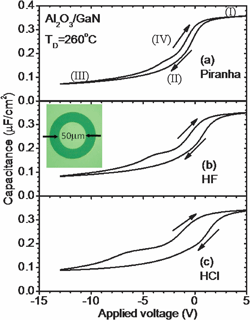
Capacitance–voltage measurements (Figure 1) showed a larger hysteresis for the sample pre-treated with hydrochloric acid, confirming that the non-uniform nucleation did indeed result in higher trap and fixed charge densities.
Figure 1: Capacitance–voltage curves of Al2O3 on n-GaN for (a) piranha, (b) HF, and (c) HCl surface treatments at deposition temperature of 260°C. Inset of (b) shows microscope image of 50μm diameter capacitor.
The researchers calculated a dielectric constant for their Al2O3 film of ~8.9 (with piranha pre-treatment). The behavior at the flat-band voltage was used to quantify the amount of hysteresis (Table 1). The measurements suggest the presence of negative trapped charge at or near the Al2O3/GaN interface. On this measure, the piranha treatment at 260°C more than halved the trapped charge compared with hydrofluoric treatment, and almost quartered it compared with hydrochloric treatment. A similar trend was seen with 240°C treatment.
Pre-treatment |
COX (μF/cm2) |
CFB (μF/cm2) |
ε |
Hysteresis at VFB (V) |
Total trapped charge (x1012/cm2) |
Piranha |
0.357 |
0.324 |
8.9 |
0.54 |
1.2 |
HF:H2O (1:1) |
0.348 |
0.317 |
8.7 |
1.15 |
2.5 |
HCl:H2O (1:1) |
0.340 |
0.309 |
8.4 |
2.13 |
4.5 |
Table 1: Summary of oxide and flat band capacitance, dielectric constant, hysteresis at VFB, and total trapped charge density of ALD Al2O3 deposited at 260°C on n-GaN for different surface pre-treatments.
Although there are a number of possible explanations for the hysteresis, such as oxide trapped charge, interface trapped charge, and/or mobile ionized impurities, the researchers suggest that there are oxide and interface trapping states at or near the Al2O3/GaN interface that are being charged and decharged (Figure 2). X-ray photoelectron spectroscopy did not find impurity-related peaks, leading the researchers to say that it is ‘unlikely that ionized impurities contribute significantly’.
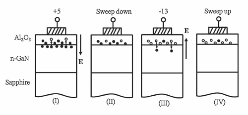
Figure 2: Schematic of electrons and their motion near the Al2O3/GaN interface due to applied bias at the (I) accumulation, (II) positive to negative bias polarity sweep (sweep down), (III) depletion, and (IV) negative to positive bias sweep (sweep up) regions. Corresponding hysteresis curve positions are marked in Figure 1(a). Closed circles represent electrons and open circles represent neutral or positive trapping states.
The researchers comment: ‘During (I) accumulation, we suspect that electrons are injected into or captured by nearby trapping states and held there during (II) the sweep from accumulation to depletion, causing a positive VFB shift. In (III) deep depletion, we suspect that the large electric field causes Poole–Frenkel or direct-tunneling electron emission from oxide and interface trapping states, resulting in a net positive shift in trapped charge. Since trap states are no longer occupied during (IV) the sweep from depletion to accumulation, VFB shifts negatively until electron injection/capture can take place again during (I) accumulation.’
On the basis of the present results, it is difficult to determine the relative contributions of oxide and surface state contributions to the trapping. However, a ‘surface-state ledge’ is seen in the hydrochloric treated sample (Figure 1(c)) that diminishes progressively with the hydrofluoric and piranha treatments.
The author Mike Cooke is a freelance technology journalist who has worked in the semiconductor and advanced technology sectors since 1997.