- News
13 January 2011
Good grades for reducing nitride LED efficiency droop
Researchers in Taiwan from National Chiao-Tung University and Epistar Co Ltd have developed a graded electron-blocking layer (GEBL) for nitride semiconductor light-emitting diodes (LEDs) that reduces efficiency droop compared with devices with a conventional EBL [C. H. Wang et al, Appl. Phys. Lett., vol97, p261103, 2010].
The efficiency droop for the GEBL LED at an injection current density of 200A/cm2 is only 4% from the peak value, compared with 34% for an LED with a conventional single composition EBL. Some of the same researchers recently used grading of multi-quantum well (MQW) structures to alleviate droop effects (Varying wells to combat LED efficiency droop).
EBLs are widely used in nitride semiconductor LEDs to confine electrons to the active light-emitting region of the device. Without an EBL, a large proportion of electrons overshoot the active region and recombine with holes in the p-type contact region of the device where they either do not produce light or they emit at a parasitic wavelength.
The EBL generally consists of aluminum gallium nitride (AlGaN) material. One problem with using such EBLs is that they also hinder the injection of holes into the active layers. Further, nitride semiconductors have large spontaneous and strain-dependent (piezoelectric) polarization electric fields that can reduced the effective barrier height of the EBL for electrons.
Some groups have explored alternative materials to AlGaN, such as aluminum indium nitride (AlInN) or AlGaInN, but these materials are presently difficult to realize and create difficulties in producing high-quality p-GaN layers.
The Taiwan-based researchers instead adopted an AlGaN EBL structure that had a varying (graded) Al content, developed using simulations (Figure 1). The aim was to reduce the electron concentration in the p-GaN region (right side of plots in Figure 1) and increase hole concentration in the multi-quantum wells (MQWs).
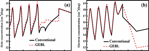
Figure 1: Calculated (a) hole concentration distribution and (b) electron concentration distribution of conventional and GEBL LEDs at a current density of 100 A/cm2.
Based on the simulations, epitaxial structures (Table 1) were grown on c-plane sapphire using metal-organic chemical vapor deposition (MOCVD). The graded EBL (GEBL) was achieved by varying the ratio of Al/Ga sources. The EBL/GEBL growth temperature was 870°C. The GEBL was graded from 0% to 25% Al. The conventional EBL contained 15% Al.
p-GaN |
contact |
200nm |
p-AlxGa1-xN EBL/GEBL |
EBL/GEBL |
20nm |
6xIn0.15Ga0.85N/GaN |
MQW |
6x(2.5nm/10nm) |
10x(InGaN/GaN) |
prestrain SL |
|
n-GaN |
contact |
4μm |
LT-GaN |
nucleation |
|
c-plane sapphire |
Table 1: Epitaxial structures grown for LEDs. (The simulations did not include pre-strain superlattice/SL layers.)
Another possible technique for grading AlGaN is temperature ramping. However, this latter method risks damaging the previous MQW structure and also creates complications due to variable growth rates.
The epitaxial material was used to create LEDs with an indium tin oxide (ITO) transparent conducting spreading layer. Nickel-gold metals were used for contacts. The mesa structures were 300μm x 300μm. Devices with graded and non-graded EBLs were tested.
Both devices had an emission wavelength around 450nm (blue) at 22A/cm2 injection current. At the same current, the forward voltage and series resistance were, respectively, 3.28V and 7Ω for the GEBL device and 3.4V and 8Ω for the conventional EBL LED. The researchers attribute the improvements for the GEBL LED to better hole injection and higher-efficiency p-type doping of the GEBL.
The light output power (L) for 30A/cm2 current injection is slightly less for the GEBL device (Figure 1). However, at higher currents the GEBL device had L values enhanced by 40% and 69% over the conventional device at 100A/cm2 and 200A/cm2, respectively.
The researchers explain the lower output at low current for the GEBL LED as being due to a high barrier at the GEBL/p-GaN interface. The holes find it difficult to tunnel through this barrier into the MQW light-emitting region. However, at higher current the tunneling barrier becomes less significant since diffusion becomes the dominant flow mechanism. Improved confinement of the electron carriers also makes a contribution to improved light output at high current.
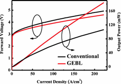 The peak efficiencies occurred at injection current densities of 80A/cm2 and 20A/cm2 for the GEBL and conventional EBL LEDs, respectively. Further, the fall-offs in efficiency (droop) at 200A/cm2 were 4% and 34% from their peak values for the GEBL and conventional EBL LEDs, respectively (Figure 2). These improvements are again attributed to better hole injection and electron confinement, ‘especially at high current density’.
Figure 2: Forward voltage and output power as a function of current density for conventional and GEBL LEDs.
National Chiao-Tung University Epistar EBL LED efficiency droop
The author Mike Cooke is a freelance technology journalist who has worked in the semiconductor and advanced technology sectors since 1997.