- News
6 April 2011
Tantalum-based ohmic contacts for nitride semiconductor transistors
Sweden’s Chalmers University of Technology and United Monolithic Semiconductors (UMS, a joint venture between Thales and EADS with production facilities in Orsay, France and Ulm, Germany) have been developing an alternative ohmic metal contact scheme based on tantalum (Ta) for use with aluminum gallium nitride (AlGaN) for high-electron-mobility transistors (HEMTs) [A Malmros et al, Semicond. Sci. Technol., vol26, p075006, 2011]. Overall, the minimum contact resistances (Rc) found for ohmic contacts with low- and high-potential-barrier epitaxial materials were 0.06Ω-mm and 0.28Ω-mm, respectively.
GaN HEMTs have potential applications for devices operating at high temperature, frequency and power density. Low-resistance contacts are needed for such devices to reduce losses and self-heating.
Conventional ohmic contacts in GaN HEMTs use titanium (Ti) and aluminum (Al), along with a cap to avoid oxidation of the Al layer. The cap often consists of nickel (Ni) or Ti with gold (Au). These structures require annealing at temperature around 800°C, which can damage the performance of the semiconductor heterostructure on which the HEMT action depends. These temperatures can also melt Al, creating unwanted surface roughness of the contact.
Alternative ohmic metals for use with nitride semiconductors are being sought using molybdenum or Ta, for example, which can be annealed at lower temperatures.
The Chalmers/UMS researchers used transmission line method (TLM) structures, which are commonly used to determine the contact resistance of metal–semiconductor junctions. The TLM structures were placed on two particular epitaxial materials grown using metal-organic chemical vapor deposition (MOCVD) on silicon carbide substrates (Table 1). Such epitaxial structures are used for HEMT development.
Epi I |
Epi II |
|
Cap |
GaN, 3 nm |
– |
Barrier |
Al0.14Ga0.86N, 22 nm |
Al0.25Ga0.75N, 25 nm |
Buffer |
GaN |
GaN |
Table 1: Epitaxial heterostructures used in the experiments.
The wafers were diced into pieces measuring 16mm x 16mm before the contact metal deposition. The surfaces were prepared by degreasing, cleaning and etching into mesas. The contacts were created using photolithographic patterning and metal evaporation. The metalized samples were diced further before different anneal treatments were performed.
A variety of sample structures were produced (Table 2) in two main groups with Ta/Al/Ni/Au (samples 1–4) and Ta/Al/Ta (6–17) metallization schemes. The second group (samples 6–17) was produced with the aim of creating a simpler structure and facilitating better understanding of the contact formation. The final Ta layer in the second group is used to prevent oxidation of the Al. A traditional Ti/Al/Ni/Au (sample 5) scheme was also produced for comparison purposes.
Layer thickness ( Å) |
|||||||||
Sample |
Ti |
Ta |
Al |
Ta |
Ni |
Au |
Thickness ratio |
Epi |
Min. Rc (Ω-mm) |
1 |
– |
100 |
700 |
– |
400 |
400 |
7 |
I |
1.36 |
2 |
– |
100 |
1200 |
– |
400 |
400 |
12 |
I |
1.75 |
3 |
– |
100 |
1400 |
– |
400 |
400 |
14 |
I |
0.41 |
4 |
– |
100 |
2800 |
100 |
– |
500 |
28 |
I |
2.23 |
5 |
200 |
– |
1100 |
– |
400 |
400 |
– |
I |
1.63 |
6 |
– |
100 |
700 |
200 |
– |
– |
7 |
I |
0.63 |
7 |
– |
100 |
1400 |
200 |
– |
– |
14 |
I |
0.26 |
8 |
– |
100 |
2100 |
200 |
– |
– |
21 |
I |
0.65 |
9 |
– |
100 |
2800 |
200 |
– |
– |
28 |
I |
0.06 |
10 |
– |
100 |
700 |
200 |
– |
– |
7 |
II |
0.47 |
11 |
– |
100 |
1400 |
200 |
– |
– |
14 |
II |
0.54 |
12 |
– |
100 |
2100 |
200 |
– |
– |
21 |
II |
0.42 |
13 |
– |
100 |
2800 |
200 |
– |
– |
28 |
II |
0.28 |
14 |
– |
50 |
2800 |
200 |
– |
– |
56 |
I |
0.25 |
15 |
– |
200 |
2800 |
200 |
– |
– |
14 |
I |
0.49 |
16 |
– |
50 |
2800 |
200 |
– |
– |
56 |
II |
0.42 |
17 |
– |
200 |
2800 |
200 |
– |
– |
14 |
II |
1.45 |
Table 2: List of fabricated samples and the minimum Rc achieved.
The annealing of samples was performed in an AG Heatpulse 610 rapid thermal processor (RTP) in nitrogen. Optimization of the anneal temperature was first carried out with a constant duration of 60s.
The minimum contact resistance of 0.41Ω-mm for the first group of samples (1–4) occurred with sample 3 at an annealing temperature of 550°C. These results are very sensitive to the Al layer thickness, which makes process control, and hence manufacturing, difficult. The comparison stack (sample 5) became ohmic at 625°C with a minimum contact resistance of 1.63Ω-mm. These results were all obtained with the ‘epi I’ structure with a 14%-Al AlGaN barrier and 3nm GaN cap layer.
The same epi I structure with Ta/Al/Ta metallization (samples 6–9) showed much less sensitivity to the Al layer thickness. The best value of contact resistance of 0.06Ω-mm for sample 9 was achieved with an annealing temperature of 550°C.
Samples 10–13 on the epi II structure, with 25%-Al AlGaN barrier and no GaN cap, exhibited the lowest contact resistance of 0.42Ω-mm at 600°C. In the last sequence of samples (14–17), where the bottom Ta layer thickness was varied, the minimum contact resistance was also achieved at 600°C.
From this point, the researchers focused on the stack without Ni-Au, seeing the use of these metals as being an ‘unnecessary, complicating factor’.
The anneal duration was then varied at a temperature of 550°C (Figure 1). The results suggest that the epi II structure requires longer duration to anneal the Ta/Al/Ta stack.
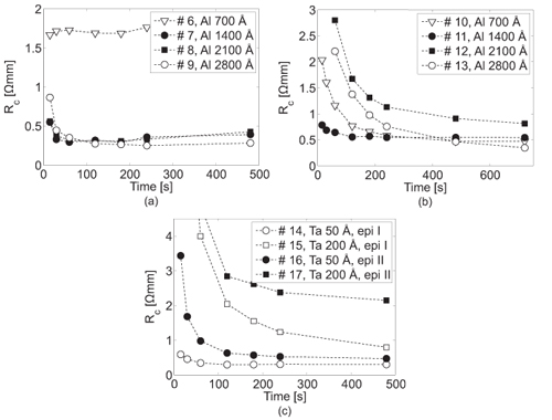
Figure 1: Rc versus time of annealing at 550°C for samples 6–17: (a) Ta/Al/Ta metallization on epi I, (b) Ta/Al/Ta metallization on epi II and (c) Ta/Al/Ta metallization on epi I and II with different Ta layer thicknesses.
On the basis of comparing the minimum contact resistances with the thickness ratios for the Ta and Al ratios, the researchers comment: “Both heterostructures exhibited the minimum Rc at a tAl/tTa of 28, which may indicate that this value is close to optimum”. However, they also believe that more work is needed to confirm this.
The researchers also studied the sheet resistance of the epitaxial material, which needs to be maintained for transistor performance. The value remained stable at 980Ω/square for epi I up to 575°C. Epi II maintained its sheet resistance to higher anneal temperatures — sample 11 had an increase in sheet resistance from its normal value of 420Ω/square to 500Ω/square after annealing at 650°C for 60secs.
SEM and optical analysis showed smooth surfaces of the metal layers up to 600°C. At higher temperatures the surface morphology became rougher. Smoother morphology would facilitate lateral scaling/size reduction of devices.
Further work involved transmission electron microscopy (TEM) and energy-dispersive x-ray (EDX) spectroscopy. These studies suggested that interdiffusion of metals with Ta/Al/Ni/Au metallization caused the poor performance of this sequence. On the basis of their analysis, the researchers believe that the contact mechanism is due to the formation of a metal-nitrogen compound at the metal–semiconductor interface, causing donor-like nitrogen vacancies in the semiconductor.
Thermal stability of the contacts was studied by storing samples 7 and 9 in air at 300°C. They maintained their initial contact resistance values for more than 400 hours. However, there was an increase in the epi structure sheet resistance of 6–8% over the test period.
The research was carried out as part of Sweden’s Microwave Wide Bandgap Technology project financed by Swedish Governmental Agency of Innovation Systems (VINNOVA), the Swedish Energy Agency, Chalmers University of Technology, Ericsson AB, Furuno Electric Co Ltd, Infineon Technologies Nordic AB, Norse Semiconductor Laboratories AB, Norstel AB, NXP Semiconductors BV, and Saab AB. United Monolithic Semiconductors (UMS) and the Fraunhofer Institute for Applied Solid State Physics (IAF) supplied materials for the study.
Polarization junctions increase nitride transistor breakdown voltage
Chalmers University UMS Ohmic metal contact Tantalum AlGaN HEMTs
The author Mike Cooke is a freelance technology journalist who has worked in the semiconductor and advanced technology sectors since 1997.
Join Semiconductor Today's LinkedIn networking and discussion group