| Home | About Us | Contribute | Bookstore | Advertising | Subscribe for Free NOW! |
| News Archive | Features | Events | Recruitment | Directory |
News
9 September 2010
BeZnCdSe pure-green 545nm laser with threshold current density of 1.7kA/cm2
Researchers in Japan have produced low-threshold-current green laser diodes using elements from groups II and VI of the periodic table, namely beryllium (Be), zinc (Zn) and cadmium (Cd) group II and selenium (Se) from group VI [Jun-ichi Kasai et al, Appl. Phys. Express, vol3, p091201, 2010].
Although research into II-VI semiconductor blue and green light-emitting devices has a long history, it has become eclipsed in recent times by the nitride III-V semiconductors using gallium (Ga), indium (In) and aluminum (Al).
A particular problem for II-VIs is creating long lifetimes for the resulting devices. It is hoped that using Be in such structures will increase device lifetimes because the resulting materials have a higher degree of ‘covalency’ in their chemical bonds. Higher ionicity (i.e. the opposite of covalency) in nitride devices leads to high spontaneous and piezoelectric (strain-dependent) polarization electric fields that can degrade emission efficiency.
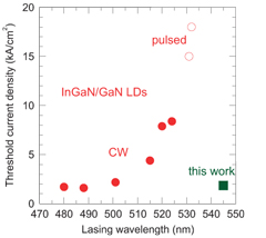
 Figure 1: Threshold current density vs lasing wavelengths as achieved by various groups using InGaN LDs and (square) the new BeZnTeSe device. Solid and open circles: continuous- and pulsed-wave, respectively.
Recently, nitride semiconductors have been used to create longer-wavelength devices than the blue–violet comfort zone by increasing the indium content of the quantum wells. However, there is a series of problems with such devices, such as efficiency droop in light-emitting diodes and relatively high threshold currents in laser diodes (Figure 1). The longest laser wavelengths for nitride lasers (~530nm) have been achieved with pulsed operation that is used to avoid self-heating effects. Continuous operation would be wanted for applications.
Green laser diodes are particularly desired for display devices. Presently, green laser light in overhead projectors uses inefficient frequency doubling of infrared laser light from semiconductor diode sources. Nitride researchers are struggling to fill this green gap with efficient direct LD emitters.
The researchers from Japan’s National Institute of Advanced Industrial Science and Technology (AIST), Hitachi and Sony have used their II-VI technology to produce low lasing current density thresholds of just 1.7kA/cm2 with a pure green emission wavelength of 545nm.
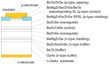
The laser diode structure (Figure 2) was grown on (001) n-type gallium arsenide (n-GaAs) substrates using molecular beam epitaxy (MBE). The silicon-doped n-GaAs III-V buffer layer was grown in a separate chamber from the remaining II-VI layers. The latter were grown using elemental material in the effusion cells of the MBE machine. The n- and p-type doping came from zinc chloride (ZnCl2 ) and nitrogen, respectively.

Figure 2: Schematic of BeZnCdSe QW laser diode.
The researchers used a separate confinement heterostructure (SCH) to provide optical confinement. The active layer consisted of a single well of BeZnCdSe material in an optical waveguide consisting of BeZnSe.
As is often the case with compound semiconductors, the p-type doping is more complicated than that for n-type material. A short-period superlattice (SPSL) consisting of a series of layers of RF-plasma-activated nitrogen-doped BeMgZnSe and ZnSe was used to achieve a higher p-type carrier concentration of 2x10¹⁷ /cm2 , as estimated from capacitance–voltage measurements. The energy bandgap in the cladding layers was ~2.85eV (~435nm, blue–violet).
A BeTe buffer layer was used to reduce defects extending from the II-VI/GaAs interface into the laser diode structure. Such defects tend to damage laser diode performance. An ohmic p-type contact was formed using a nitrogen-doped BeTe/ZnSE pseudo-graded superlattice.
The quality of the crystal layers that were produced was evaluated using high-resolution x-ray diffraction. Rocking curve measurements showed that the cladding and optical waveguide layers deviated from the base GaAs crystal structure by less than 0.1%. The quantum-well lattice mismatch was 2.2%. The SPSL satellites in the rocking curve are described as ‘sharp’, indicating successful growth.
Gain-guided laser diodes were constructed from the epitaxial material. Two groups of laser diodes were constructed: one with 5 micron-wide cap and contact mesas; the other, with 2 micron-wide structures, was designed to reduce the width of the current path. The p-type contact metal layers were titanium/platinum/gold and the n-type layers were gold-germanium and gold. The cavity was 800 microns long. The facets were coated with high-reflectivity dielectric. The laser diodes were mounted on copper heat-sinks, n-side down.
Continuous wave (CW) operation resulted in laser operation with a threshold current of 68mA and forward voltage of 10.4V for 5 micron-wide devices. This corresponded to a threshold current density of 1.7kA/cm2 . For the 2 micron-wide laser diode, the threshold decreased to 52mA.
The abruptness of the light output power at threshold suggests that the BeZnCdSe QW layer was not uniform in composition. It is believed that this is the result of the selenium source in the MBE machine being a Knudsen cell, which does not allow adequate optimization of the II/VI beam pressure ratio. The researchers suggest that a valved effusion cell could improve material quality.
There were also some kinks in the light output curve with increased current, possibly arising from the gain guiding structure being slightly wider than desired. The light output power is about 19mW at 100mA in the 5 micron laser diodes.
The forward voltage is about twice as high as that achieved in 1998 for blue–green ZnCdSe LDs (5.3V). The researchers believe that the forward voltage of their green LD could be improved using an optimized BeTe/ZnSe pseudo-grading.
The researchers point out that room-temperature CW operation of ZnCdSe/ZnSe/ZnMgSSe single-QW SCH LDs at a wavelength of 524 nm with a threshold current density of 1.4kA/cm2 was achieved in 1993. Using their own system, they envisage that reducing the cadmium content in the well could reduce the strain in the active layer, giving shorter-wavelength devices without increasing the threshold current.
See related items:
Quantum wells with AlGaN barriers increases blue-green laser light output
Nichia to ship sample green laser diodes from August
Yet another angle on nitride laser diodes
![]() Search: Green lasers
Search: Green lasers
Visit: http://apex.ipap.jp/link?APEX/3/091201
For more on green laser: Latest issue of Semiconductor Today
The author Mike Cooke is a freelance technology journalist who has worked in the semiconductor and advanced technology sectors since 1997.