| Home | About Us | Contribute | Bookstore | Advertising | Subscribe for Free NOW! |
| News Archive | Features | Events | Recruitment | Directory |
News
26 October 2010
Free-standing GaN substrate improves nitride solar cell performance
Researchers from Meijo and Nagoya universities have used free-standing gallium nitride (GaN) substrates to create nitride semiconductor solar cells with higher open-circuit voltage and fill-factor compared with devices grown on sapphire [Yosuke Kuwahara et al, Appl. Phys. Express, vol3, p111001, 2010].
One well-known effect of using free-standing GaN substrates to create nitride semiconductor devices is improved material quality, reducing parasitic resistance effects. Such devices can also use ‘vertical’ conduction arrangements with n- and p-electrodes on the top and bottom of the chip, rather than the ‘horizontal’ arrangement needed with insulating sapphire, where the two electrodes have to be on the conducting nitride side of the component.
In theory, gallium indium nitride (GaInN) semiconductors should be able to cover the range of solar photons from infrared 1.9μm wavelengths (0.65eV) with InN up to 365nm near-ultraviolet with GaN (3.4eV). In reality, GaInN is difficult to grow with large In molar fraction.
The researchers tested devices with In ~10%. The devices that were produced had photoluminescence peaks around the violet wavelength 390nm. Unfortunately, this only covers a small part of the solar power spectrum. More efficient solar cells have bandgaps in the range 1–2eV that can pick up photons from the visible range where the spectrum peaks.
The short-wavelength nitride solar cells produced by Meijo/Nagoya are thus not ideal for the spectrum of solar radiation. Hence the conversion efficiencies seen are limited to a few percent. In August, Texas Tech researchers reported nitride solar cells on sapphire with higher In molar fractions of ~35%, giving longer wavelength coverage, that had conversion efficiencies up to 3.03% when subjected to 30-sun illumination.
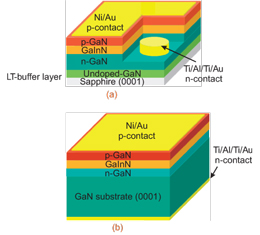 Figure 1: (a) GaInN-based solar cell with thick
u-Ga0.89In0.11N (250 nm) layer on sapphire substrate covered with low-temperature-deposited (LT) buffer layer and (b) GaInN-based solar cell with thick
u-Ga0.90In0.10N (250 nm) layer on free-standing GaN substrate.
Figure 1: (a) GaInN-based solar cell with thick
u-Ga0.89In0.11N (250 nm) layer on sapphire substrate covered with low-temperature-deposited (LT) buffer layer and (b) GaInN-based solar cell with thick
u-Ga0.90In0.10N (250 nm) layer on free-standing GaN substrate.
Meijo/Nagoya produced two devices grown in the (0001) ‘c-plane’ direction (Figure 1): one on an undoped GaN-on-sapphire layer, the other on free-standing GaN. The researchers found that using free-standing GaN reduced dislocation densities from ~109/cm3 on sapphire to ~107/cm2 with the free-standing material. The growth technique was metal-organic chemical vapor deposition (MOCVD).
The n-type layers were 2μm thick, and the undoped GaInN were 250nm. The p-GaN layers had carrier concentrations of 3.6x10¹⁸/cm3. The thickness was 100nm on the free-standing GaN and 50nm on the sapphire substrate. The researchers estimated that 92% of sunlight with photon energies above the GaInN bandgap could be absorbed in the GaInN layer.
Ohmic semi-transparent p-contacts consisting of nickel-gold were deposited and annealed. The transparency was found to be about 67% for 370nm wavelengths. The n-contacts consisted of titanium-aluminum-titanium-gold. For the free-standing GaN one could apply the contact to the back-surface, since the material was n-type conducting (4.5x10¹⁸/cm3 carrier concentration). The use of a back-contact allows a vertical conduction scheme. Since sapphire is insulating, for the comparison device a separate horizontal conductive structure was needed. Neither device had anti-reflective coatings to improve photon collection.
A variety of material characterizations were carried out: x-ray diffraction (XRD), transmission electron microscopy (TEM) and microscopic photoluminescence. The external quantum efficiency (EQE) was calculated using the photocurrent under excitation by a xenon lamp in a spectroscope.
From the x-ray diffraction study, the researchers determined that the In molar fraction for the GaInN layers was 0.10 and 0.11 for the free-standing GaN and sapphire devices, respectively. It was also found that the GaInN layer crystal structure were less twisted, tilted and dislocated on the free-standing GaN.
The devices were tested for photovoltaic power generation in a solar simulator with an air mass index of AM1.5 and 1.5-sun intensity at room temperature (Table 1). The open-circuit current with the free-standing GaN device is described as ‘low’, with the sapphire device having a slightly higher value. The researchers think this could be due to the thicker p-GaN layer used (100nm) for the free-standing device, making it harder for the light to get through to the active GaInN layer.
Device performance |
Sapphire substrate |
GaN substrate |
Max. EQE (%) |
55 |
55 |
EL peak wavelength (nm) |
394 |
388 |
Rsh (Ω-cm2) |
3.47x10³ |
2.33x10⁴ |
Rs ( Ω-cm2) |
1.39x10² |
1.38x10² |
Jsc (mA/cm2) |
1.82 |
1.59 |
Voc (V) |
1.62 |
2.23 |
Fill factor (%) |
52 |
61 |
Conversion efficiency (%) |
0.98 |
1.41 |
Table 1: Device performance characteristics of nitride-based solar cells on sapphire and GaN substrates. Rs = series resistance, Rsh = shunt resistance.
Although both devices have a maximum EQE of 55% at 370nm, the free-standing GaN device has a lower total EQE due to absorption in the p-GaN layer below 365nm. The researchers estimate the internal quantum efficiency (IQE) at 82%, close to the theoretical maximum of 92%.
The free-standing GaN device did perform better in terms of open-circuit voltage (1.4x) and fill factor (1.2x). The fill factor expresses the maximum output power as a fraction of the product of Voc and Isc. These higher values are attributed to the better-quality material growth that was enabled by use of a free-standing GaN substrate.
New Energy and Industrial Technology Development Organization Project, Research and Development on Innovative Solar Cells provided partial support for the research.
See related items:
Texas Tech ‘significantly’ improves InGaN solar cell performanceProgress towards high-efficiency InGaN/Si tandem solar cell
![]() Search: Nitride solar cells Free-standing GaN substrates
Search: Nitride solar cells Free-standing GaN substrates
Visit: http://apex.jsap.jp
For more: Latest issue of Semiconductor Today
The author Mike Cooke is a freelance technology journalist who has worked in the semiconductor and advanced technology sectors since 1997.
![]() ©2010 Juno Publishing and Media Solutions Ltd. All rights reserved. Semiconductor Today and the editorial material contained within it and related media is the copyright of Juno Publishing and Media Solutions Ltd. Reproduction in whole or part without permission from Juno Publishing and Media Solutions Ltd is forbidden. In most cases, permission will be granted, if the author, magazine and publisher are acknowledged.
©2010 Juno Publishing and Media Solutions Ltd. All rights reserved. Semiconductor Today and the editorial material contained within it and related media is the copyright of Juno Publishing and Media Solutions Ltd. Reproduction in whole or part without permission from Juno Publishing and Media Solutions Ltd is forbidden. In most cases, permission will be granted, if the author, magazine and publisher are acknowledged.
Disclaimer: Material published within Semiconductor Today and related media does not necessarily reflect the views of the publisher or staff. Juno Publishing and Media Solutions Ltd and its staff accept no responsibility for opinions expressed, editorial errors and damage/injury to property or persons as a result of material published.
Semiconductor Today, Juno Publishing and Media Solutions Ltd, Suite no. 133, 20 Winchcombe Street, Cheltenham, GL52 2LY, UK
Web site by No Name No Slogan ![]()