| Home | About Us | Contribute | Bookstore | Advertising | Subscribe for Free NOW! |
| News Archive | Features | Events | Recruitment | Directory |
News
6 October 2010
Fujitsu develops record 1.3W output W-band GaN HEMT power amplifier
At this week’s 2010 IEEE Compound Semiconductor IC Symposium (CSICS) in Monterey, CA, USA (3–6 October), Japan’s Fujitsu Laboratories Ltd is presenting its development of a power amplifier using gallium nitride (GaN) high-electron-mobility transistors (HEMTs) that has achieved record power output of 1.3W for wireless communications in the millimeter-wave W-band (75–110GHz), for which widespread usage is expected in the future (e.g. for applications including high-speed wireless communications, automotive radar, and image sensors). The new amplifier can offer output equivalent to about 16 times that of existing amplifiers using gallium arsenide, enabling W-band transmission ranges to be extended by about six times.
Fujitsu says that the new GaN HEMT-based power amplifier will make high-capacity wireless communications possible in regions in which it is unfeasible to lay optical fiber cables, in addition to ensuring high-quality communications in rain and under other conditions where the millimeter-wave signal is known to attenuate.
Part of the research was conducted under contract as part of the ‘Research and Development Project for Expansion of Radio Spectrum Resources’ of Japan’s Ministry of Internal Affairs and Communications.
To accommodate the demands for greater bandwidth resulting from increases in Internet communications and expansions in mobile phone networks, optic fiber cables are being laid in nations throughout the world to create a high-capacity trunk-line system. Fujitsu says that this is problematic in areas with challenging topography, sparking interest in high-bandwidth wireless trunk lines capable of data transmission capacities up to 10Gbps — on a par with fiber-optic cabling — as a way to bridge what Fujitsu calls the ‘digital divide’ for wireless communications.
The millimeter-wave W-band is an effective band for wireless communications at speeds of up to 10Gbps, as it is readily available (see wireless transceiver employing millimeter-wave W-band in Figure 1). The power amplifier inside a transmitter is the key component for amplifying the millimeter-wave signal to the intensity required for transmission.
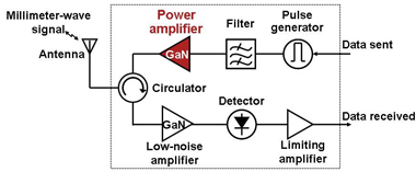
Figure 1: Millimeter-wave W-band transceiver (example of impulse radio).
Up until now, Fujitsu and Fujitsu Laboratories have produced 350mW of power using power amplifiers based on GaN HEMTs. However, the W-band experiences significant signal attenuation due to factors such as atmospheric absorption and rain, and there has been demand for high-output power amplifiers that can transmit a stable signal across distances ranging from a few kilometers to several tens of kilometers.
Fujitsu says that, to develop a high-output W-band power amplifier, the following issues had to be addressed:
- Transistor operating speed (operating frequency) is determined by the speed at which electrons pass directly beneath the gate electrodes. To operate at high frequency (e.g. the millimeter-wave band) the length of the gate electrodes must be decreased. On the other hand, an effective method of achieving high power output is applying a high voltage to the transistor. But, when the GaN HEMT gate length is reduced and the transistor is operated at a high voltage, electrons increase speed dramatically, and hence some of them can leak from the current pathway (electron channel layer), reaching the passivation layer, where they accumulate (Figure 2). There is hence a reduction in electrons contributing to high-frequency operation (a loss in high-frequency current), making it difficult to increase power output.
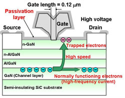 Figure 2: Cross section of millimeter-wave GaN HEMT transistor.
- Power distribution within a power amplifier is performed by dividing the input signal among multiple parallel transistors in the power splitter circuit. After the signal is amplified by each transistor, it is combined again using the combiner circuit, enabling high power output (Figure 3). But at frequencies above 70GHz, due to the interference of high-frequency complex signal distribution, the signal undergoes attenuation in the power splitter and combiner circuits. It was hence necessary to construct a power splitting and combination model for use in the millimeter-wave band, and to develop a design that takes the complex signal distribution into consideration while enabling the desired output to be achieved.
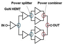 Figure 3: Structure of millimeter-wave W-band amplifier.
To resolve these issues, Fujitsu therefore developed the following technologies:
- Optimizing the GaN HEMT passivation layer. After analyzing why electrons escaped from the electron channel layer and accumulated in the passivation layer, Fujitsu traced the issue to the existence of defects in the crystallization of the silicon nitride (SiN) used as part of the passivation layer. By enhancing the layer's SiN composition and crystalline structure, Fujitsu fabricated a passivation layer with minimal crystalline defects, making it difficult for electrons to accumulate. The new technology able to amplify high-frequency current to more than two times the power of existing technology.
- Building a power division and combination model through electromagnetic analysis. By performing electromagnetic analysis on the complex signal distribution of the high-frequency signal, based on the physical properties of the power splitter and combiner circuits, Fujitsu designed a highly precise circuit that reduces signal attenuation in the two circuits. Fujitsu was hence able to increase design precision by about 15%.
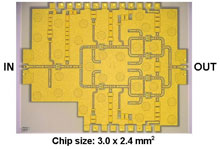
Figure 4 (a and b): New GaN HEMT amplifier and its characteristics.
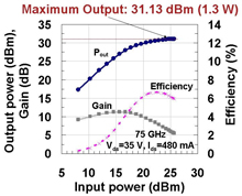
The above technologies were used to develop a power amplifier for millimeter-wave W-band wireless equipment that achieved a maximum output of 1.3W which, among GaN HEMT power amplifiers, represents the highest output in this frequency band using a single integrated circuit, it is claimed.
The new technology also achieves transmission output equivalent to 16 times that of existing amplifiers using GaAs. Employed in combination with the GaN HEMT receiver amplifier developed by Fujitsu last year, it is expected that transmission ranges can be extended by about six times compared to GaAs-based transceivers. The firm says that this should enable millimeter-wave wireless communications equipment to be deployed in a wider range of fields, while ensuring high-quality communications in which ample signal output can be obtained even when there is signal attenuation due to rain and other factors.
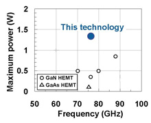 Figure 5: Comparison with other millimeter-wave W-band amplifiers.
Fujitsu and Fujitsu Laboratories plan to work to further improve the performance and expand the frequency spectrum of the GaN HEMT power amplifier, while employing the technology in a wide range of applications, including millimeter-wave-enabled trunk lines and ultra-high-speed wireless network access.
See related items:
Fujitsu doubles output record to 12.9W for C-Ku band GaN HEMT amplifiers
![]() Search: Fujitsu W-band PA GaN HEMT
Search: Fujitsu W-band PA GaN HEMT
Visit: http://jp.fujitsu.com/labs/en
For more: Latest issue of Semiconductor Today
![]() ©2010 Juno Publishing and Media Solutions Ltd. All rights reserved. Semiconductor Today and the editorial material contained within it and related media is the copyright of Juno Publishing and Media Solutions Ltd. Reproduction in whole or part without permission from Juno Publishing and Media Solutions Ltd is forbidden. In most cases, permission will be granted, if the author, magazine and publisher are acknowledged.
©2010 Juno Publishing and Media Solutions Ltd. All rights reserved. Semiconductor Today and the editorial material contained within it and related media is the copyright of Juno Publishing and Media Solutions Ltd. Reproduction in whole or part without permission from Juno Publishing and Media Solutions Ltd is forbidden. In most cases, permission will be granted, if the author, magazine and publisher are acknowledged.
Disclaimer: Material published within Semiconductor Today and related media does not necessarily reflect the views of the publisher or staff. Juno Publishing and Media Solutions Ltd and its staff accept no responsibility for opinions expressed, editorial errors and damage/injury to property or persons as a result of material published.
Semiconductor Today, Juno Publishing and Media Solutions Ltd, Suite no. 133, 20 Winchcombe Street, Cheltenham, GL52 2LY, UK
Web site by No Name No Slogan ![]()